Inductor built-in wiring board having shield function

a built-in wiring board and function technology, applied in the direction of cross-talk/noise/interference reduction, electrical apparatus construction details, support structure mounting, etc., can solve the problems of complex component management, difficult to reduce the size of a device, and the reliability of mounting components. achieve the effect of large inductance value and easy securement of an area

Active Publication Date: 2009-01-08
SHINKO ELECTRIC IND CO LTD
View PDF5 Cites 34 Cited by
  • Summary
  • Abstract
  • Description
  • Claims
  • Application Information

AI Technical Summary

Benefits of technology

[0020]It is an aspect of the present invention to provide an inductor built-in wiring board, in which an inductor is formed using the shield structure shown in FIGS. 2 to 4 and the inductor is pattern-formed on a wiring board. Therefore, a wiring space is effectively used. A pattern forming area decreases in the case of obtaining an inductor by forming a coil on the wiring board. Further, a desired inductance value is obtained, and the board is capable of coping with a high resonance frequency.
[0032]According to the invention, the wiring board has a shield function by joining the convex patterns of the shield patterns with the conductive shield patterns of the wiring board and thus the inductor formed on the wiring board is shielded. Therefore, it is easy to secure an area for the inductor without generating noises from the inductor to the other electronic components. As a result, it is possible to obtain a large inductance value.

Problems solved by technology

According to the related-art method of mounding the components on the printed circuit board as described above, it is necessary to prepare the discrete coil, and thus management of components is complicated.
In addition, there might be a problem in reliability for mounting components.
Moreover, a considerable space for mounting components such as coils is necessary, and thus it is difficult to reduce a size of a device.
As a result, a size of the printed circuit board increases, and thus it is difficult to reduce the size of the device.
However, forming a coil on a printed wiring board, it is difficult to obtain a reasonably satisfactory inductor in light of a pattern forming area, an inductance value, a resonance frequency.

Method used


Image

  • Inductor built-in wiring board having shield function
  • Inductor built-in wiring board having shield function
  • Inductor built-in wiring board having shield function

Examples


Embodiment Construction

[0044]Hereinafter, exemplary embodiments of the present invention will be described in detail with reference to the drawings.

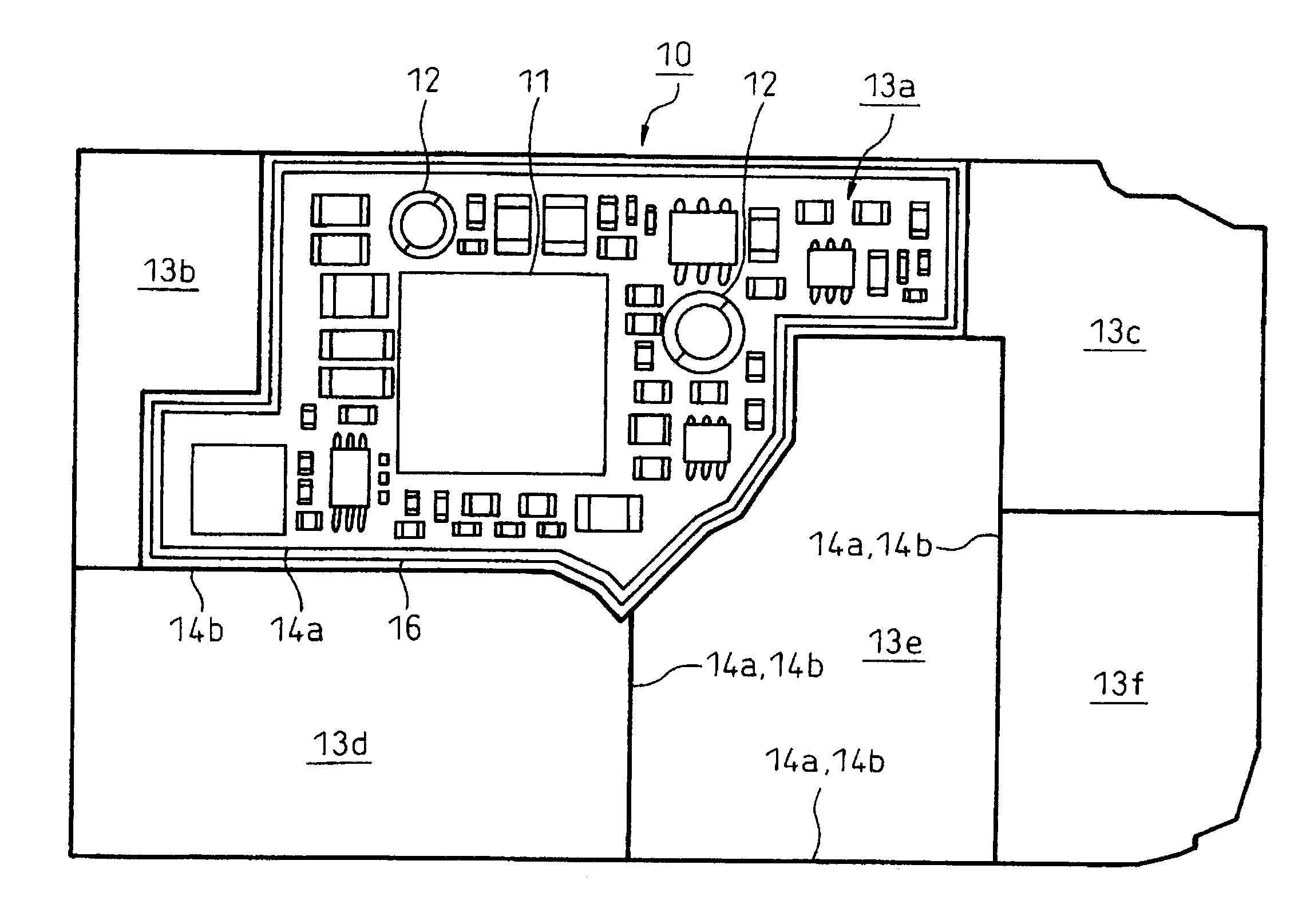
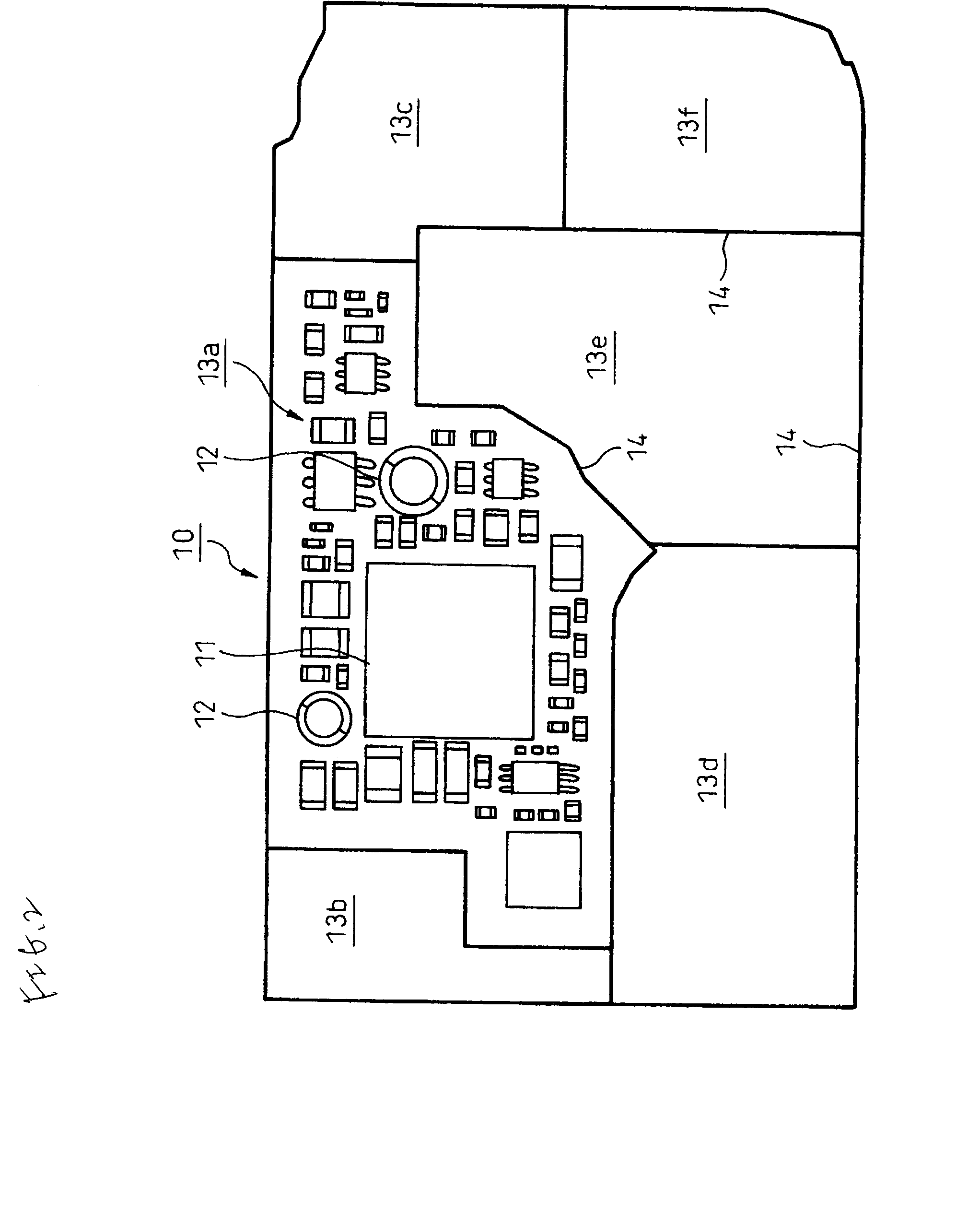
[0045]FIG. 5 is a plan view illustrating an inductor built-in wiring board having a shield function according to exemplary embodiments of the present invention. FIG. 6 is a plan view illustrating only shield patterns and a wiring of an inductor.

[0046]As shown in FIG. 5, various kinds of electronic components 11 such as semiconductor elements are mounted on a surface of a wiring board 10. These electronic components might include board mounted inductors 12. A plurality of conductive shield patterns 14a and 14b surround each circumference of circuit blocks 13a to 13f in which the same block is set as one area, and are formed on the surface of the wiring board 10. In the shown embodiment, two conductive shield patterns are formed adjacent to each other. The inner and outer circumferential two conductive shield patterns 14a and 14b are continuously formed, for exa...


PUM


Abstract

There is provided a wiring board having a shield function. The wiring board includes: a plurality of conductive shield patterns adapted to surround a circumference of at least one electronic component mounting area on the wiring board, the plurality of conductive shield patterns being adjacent to each other; and at least one inductor formed of a conductive pattern and provided between the conductive shield patterns.

Description

[0001]This application is based on and claims priority from Japanese Patent Application No. 2007-175514, filed on Jul. 3, 2007, the entire contents of which are hereby incorporated by reference.BACKGROUND[0002]1. Technical Field[0003]The present disclosure relates to a wiring board having a shield function, and more particularly, to an inductor built-in wiring board having a shield function.[0004]2. Related Art[0005]In a power supply circuit used for a cellular phone, a personal computer, a portable terminal, a PDA, a vehicle control device, a small-size communication machine, a small-size game machine, and the like, inductors (switching power supply or the like) are essential components, and the inductors are separately mounted on a printed circuit board. That is, as a general method, electronic components or electronic circuit elements are mounted on the printed circuit board, and discrete coils are soldered onto the printed circuit board when components having desired circuit fun...

Claims


Application Information

Patent Timeline
Patent Type & Authority Applications(United States)
IPC IPC(8): H05K9/00
CPCH01F2017/008H05K1/0218H05K1/0219H05K2201/10371H05K2201/09236H05K2201/09972H05K1/165
Inventor MASHINO, NAOHIRO
Owner SHINKO ELECTRIC IND CO LTD
Why Eureka
Try Eureka