Liquid crystal display device and electronic apparatus

a display device and liquid crystal technology, applied in non-linear optics, instruments, optics, etc., can solve problems such as contrast degradation, optical leakage, and display deterioration, so as to prevent or suppress electric field, and prevent liquid crystal molecules from disorienting due to electric field

Inactive Publication Date: 2009-01-08
SEIKO EPSON CORP
View PDF16 Cites 10 Cited by
  • Summary
  • Abstract
  • Description
  • Claims
  • Application Information

AI Technical Summary

Benefits of technology

[0007]An advantage of the present invention is that it provides a vertically-oriented liquid crystal display device having a configuration in which the orientation of liquid crystal molecules can be properly controlled and in which the deterioration of display, such as optical leakage, can be suppressed, and further, it provides an electronic apparatus having the liquid crystal display device.
[0008]A liquid crystal display device according to an aspect of the invention includes: a pair of substrates including an element substrate and a counter substrate; and a liquid crystal layer interposed between the pair of substrates, wherein the liquid crystal layer is composed of liquid crystals each having a negative dielectric anisotropy, indicating that an initial oriented state is vertically-oriented, wherein the element substrate includes a switching element, an insulating layer formed on the switching element, and a pixel electrode formed on the insulating layer, wherein the pixel electrode has a plurality of island-shaped portions and a plurality of branch-shaped portions connecting between the plurality of island-shaped portions, and the switching element and the pixel electrode are electrically connected to each other via a contact hole formed in the insulating layer, wherein a spacer for defining the thickness of the liquid crystal layer is provided at the side of the liquid crystal layer of at least one substrate of the pair of substrates, and wherein the contact hole and the spacer are disposed at different locations on the surface of the one substrate and are provided in a region where the island-shaped portions and the branch-shaped portions of the pixel electrode are not formed.
[0009]The liquid crystal display device according to the aspect of the invention is a vertically-oriented active matrix type liquid crystal display device, in which an insulating layer (interlayer insulating layer) is formed between a switching element and a pixel electrode, so that it is possible to prevent or suppress an electric field from occurring between the switching element and the pixel electrode. As a result, the disorientation of liquid crystal molecules due to the electric field can be prevented or suppressed.
[0010]Further, the pixel electrode is constituted by a plurality of island-shaped portions and a plurality of branch-shaped portions connecting the island-shaped portions to each other, so that a gradient electric field may be generated along the periphery of the island-shaped portion between the pixel electrode and the electrode (i.e. the opposite electrode) formed on the counter substrate. As a result, it is possible to control the orientation of the liquid crystal molecules in response to the gradient electric field. Therefore, orientation division of the liquid crystal molecules can be implemented for each island-shaped portion, so that the trouble such as disorderly orientation within the pixel electrode can be prevented or suppressed.
[0011]Furthermore, in accordance with the aspect of the invention, the insulating layer is interposed between the switching element and the pixel electrode and the contact hole is formed all over the insulating layer to have the switching element and the pixel electrode electrically connected to each other as described above. However, concave shapes are often generated at the interposing surface of the liquid crystal layer in the region where the contact hole is formed, and the disorientation of the liquid crystal molecules is apt to occur due to the concave shapes. Accordingly, it is not preferable that the contact hole is formed so as to overlap the pixel electrode in plan view. Therefore, in accordance with the aspect of the invention, the contact hole is formed in a region where the island-shaped portion and the branch-shaped portion are not formed, that is, the contact hole is formed in a region which does not contribute to display. As a result, empty spaces formed between the island-shaped portions designed for the purpose of orientation division of the liquid crystal molecules can be effectively utilized, which allows unnecessary consumption of the display region to be prevented. In this case, the disorientation of the liquid crystal molecules which may occur due to formation of the contact hole occurs in a region except the region where the pixel electrode is formed, so that the disorientation can be reduced in the pixel region as compared to a case of having the contact hole formed to overlap the pixel electrode.
[0012]Moreover, in accordance with the aspect of the invention, a spacer is disposed in at least one of the pair of substrates in order to define the thickness of the liquid crystal layer. However, the disorientation of the liquid crystal molecules is apt to occur near the spacer. In this case, the spacer is also formed in a region where the island-shaped portions of the pixel electrode and the branch-shaped portions are not formed as is done with the contact hole, so that the empty space of the pixel electrode can be effectively used and adverse effects (e.g. display spot or afterimage) on the display caused by the disorientation of the liquid crystal molecules near the spacer can be decreased. As an example of the spacer used for the liquid crystal display device of the invention, there is a spacer formed by using a resin material within the substrate surface, and specifically, a photo-spacer selectively formed by using a photolithography method.

Problems solved by technology

However, in a region where the contact hole is formed, a concave-shaped inclined surface occurs at the surface of the pixel electrode, so that disorientation of the vertically-oriented liquid crystals may occur near the inclined surface.
Also, in addition to the contact hole, disorientation of the vertically-oriented liquid crystal may also occur near a spacer that defines the thickness of the liquid crystal.
The disorientation in turn causes an optical leakage, and so on, which leads to deterioration of the display, such as contrast degradation.
However, concave shapes are often generated at the interposing surface of the liquid crystal layer in the region where the contact hole is formed, and the disorientation of the liquid crystal molecules is apt to occur due to the concave shapes.
However, the disorientation of the liquid crystal molecules is apt to occur near the spacer.

Method used


Image

  • Liquid crystal display device and electronic apparatus
  • Liquid crystal display device and electronic apparatus
  • Liquid crystal display device and electronic apparatus

Examples


first embodiment

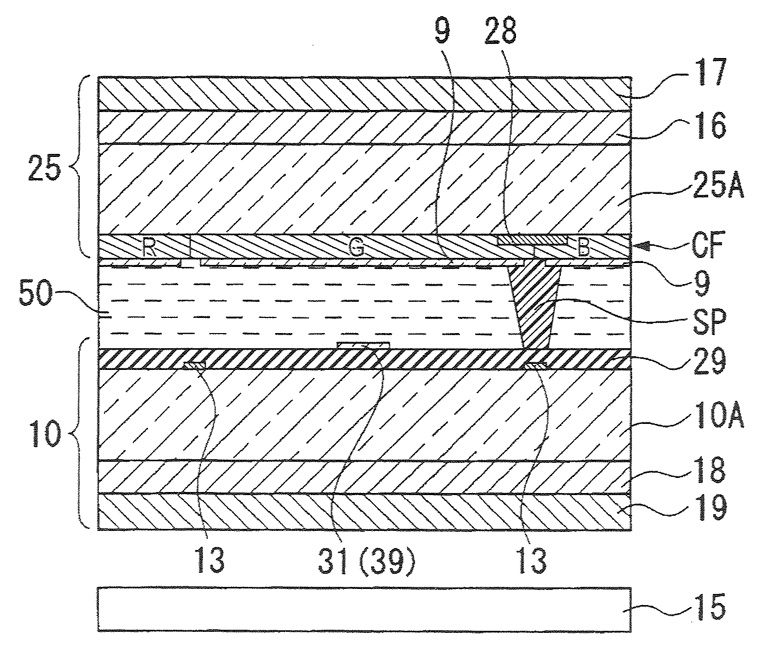
[0030]Hereinafter, a first embodiment of the present invention will be described with reference to FIGS. 1 to 4. The liquid crystal display device of the embodiment is an example of an active matrix liquid crystal display device using a thin film diode (hereinafter, referred to as a TFD) as a switching element, and in particular, it is an example of a vertically-oriented liquid crystal transmissive display device. Also, the size of each layer or each member is scaled to be different from each other in the drawings so as to allow the layer or the member to be recognizable in the drawings.

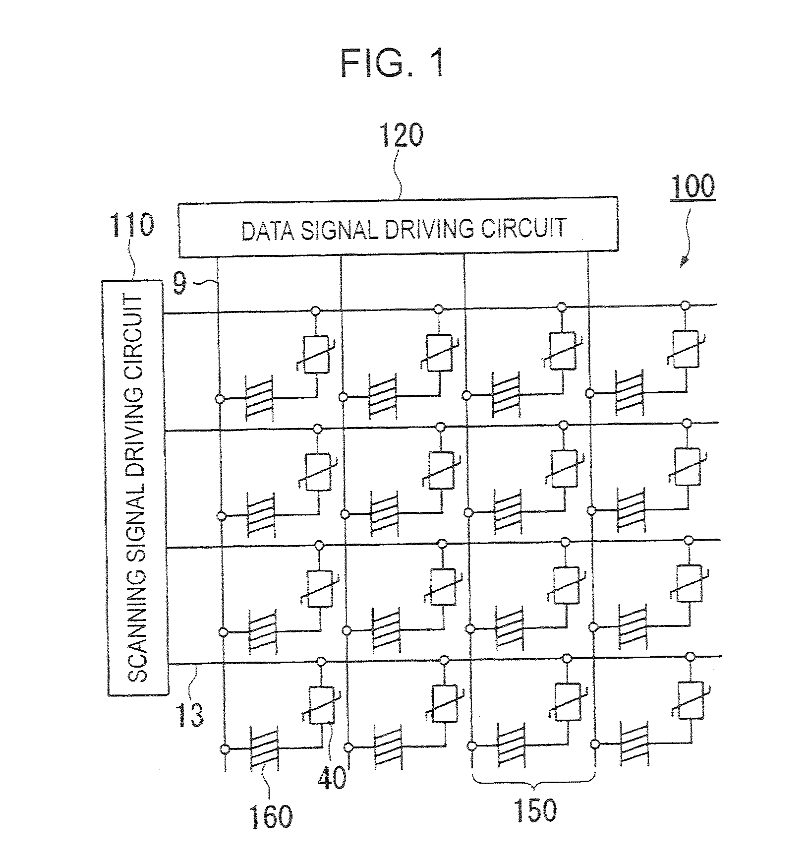
[0031]FIG. 1 is an equivalent circuit diagram illustrating the liquid crystal display device 100. The liquid crystal display device includes a scanning signal driving circuit 110 and a data signal driving circuit 120. Signal lines, that is, a plurality of scanning lines 13, and a plurality of data lines 9 intersecting with the scanning lines 13 are disposed in the liquid crystal display device 100, a...

second embodiment

[0049]Hereinafter, the second embodiment according to the invention will be described with reference to FIGS. 5 and 6. FIG. 5 is a cross-sectional view schematically illustrating the pixel configuration of the liquid crystal display device of the second embodiment, and corresponds to FIG. 3 of the first embodiment. In addition, FIG. 6 is a schematic view taken along the line B-B′ of FIG. 5, which corresponds to FIG. 4A of the first embodiment. The basic configuration of the liquid crystal display device of the second embodiment is the same as in the first embodiment, but differs from the first embodiment only in the configuration of the pixel electrode. Accordingly, in FIGS. 5 and 6, the same elements as in FIGS. 3 and 4 are denoted by the same reference numerals, and detailed explanation thereof will be omitted.

[0050]One dot region is divided into three sub-dot regions to constitute the pixel in the first embodiment; however, one dot region is divided into two sub-dot regions S1 an...

third embodiment

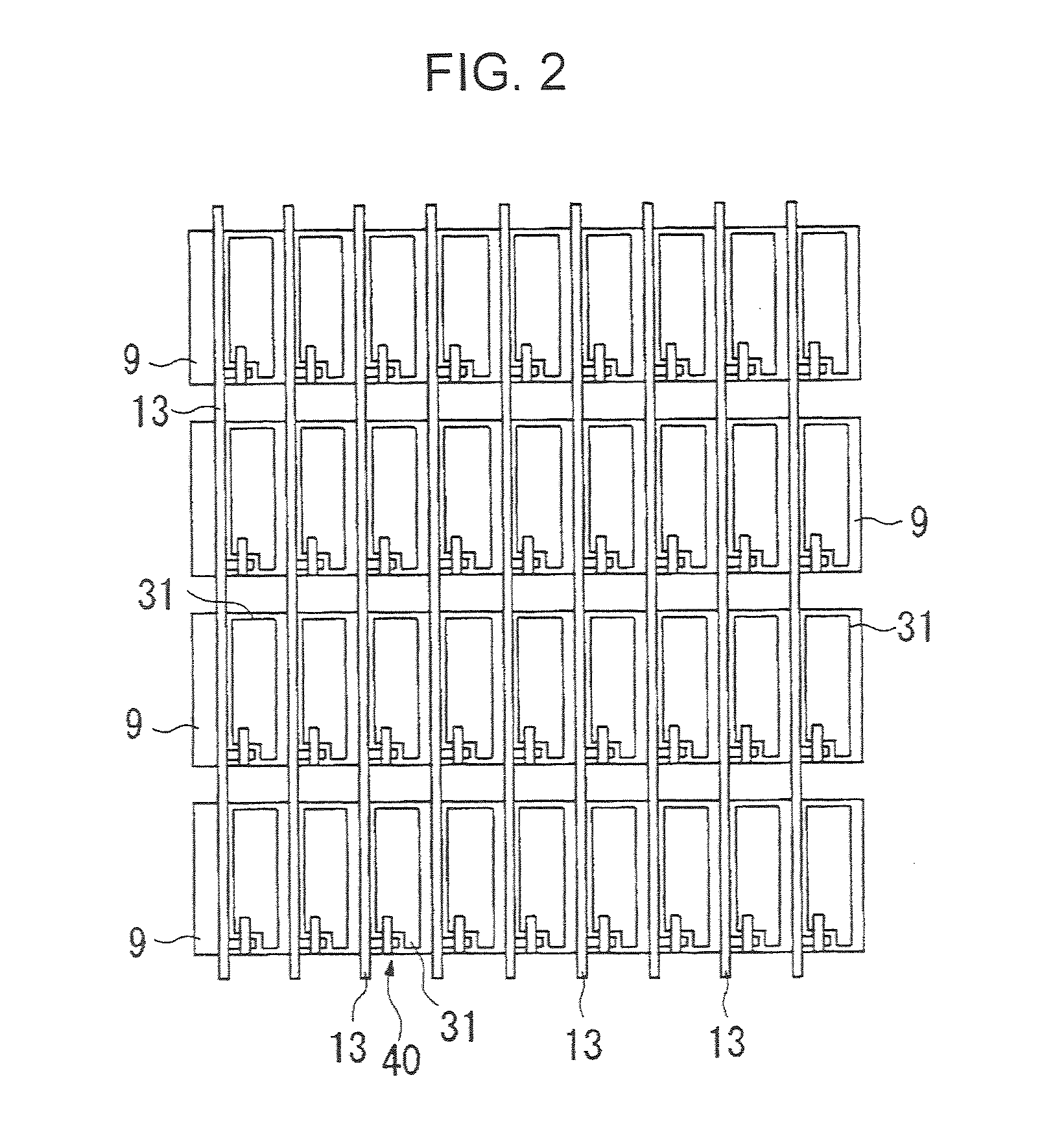
[0053]Hereinafter, the third embodiment according to the invention will be described with reference to FIGS. 7 and 8. FIG. 7 is an equivalent circuit view of the liquid crystal display device of this embodiment, and FIG. 8 is a plan view illustrating one pixel of the liquid crystal display device of the embodiment, which is a schematic view corresponding to FIG. 3 of the first embodiment. In addition, in FIG. 8, the same elements as in FIG. 3 are denoted by the same reference numerals, and detailed explanation thereof will be omitted.

[0054]The liquid crystal display device of this embodiment is an active matrix type liquid crystal display device using a thin film transistor (hereinafter, referred to as TFT) as a switching element, and also an example of a vertically-oriented liquid crystal display device.

[0055]In the liquid crystal display device of the embodiment, as shown in FIG. 7, the pixel electrodes 31 and the TFTs 30 serving as the switching elements for controlling the pixel...


PUM

PropertyMeasurementUnit
dielectric anisotropyaaaaaaaaaa
thicknessaaaaaaaaaa
electric fieldsaaaaaaaaaa

Abstract

A vertically-oriented liquid crystal display device having a configuration in which the orientation of liquid crystal molecules can be properly controlled and in which the deterioration of display, such as optical leakage, can be suppressed.

Description

CROSS-REFERENCE TO RELATED APPLICATIONS[0001]This application is a divisional patent application of U.S. Ser. No. 11 / 120,110 filed May 2, 2005, claiming priority to Japanese Patent Application No. 2004-138540 filed May 7, 2004, all of which are hereby incorporated by reference.BACKGROUND OF THE INVENTION[0002]1. Technical Field[0003]The present invention relates to a liquid crystal display device and an electronic apparatus, and more particularly, to a liquid crystal display device using vertically-oriented liquid crystals.[0004]2. Related Art[0005]Recently, vertically-oriented liquid crystal devices are utilized in liquid crystal TVs, display screens of mobile phones, and so on. An example of a vertically-oriented liquid crystal display device is disclosed, for example, in Japanese Unexamined Patent Application Publication 9-236821. Specifically, a technique is disclosed in which thin film transistors are formed and pixel electrodes are formed on an interlayer insulating layer (ove...

Claims


Application Information

Patent Timeline
Patent Type & Authority Applications(United States)
IPC IPC(8): G02F1/1339G02F1/1333G02F1/1335G02F1/1337G02F1/1343G02F1/1362G02F1/1365G02F1/1368G02F1/139
CPCG02F1/13394G02F1/1393G02F1/136227G02F1/134309G02F1/1337
Inventor HIGA, MASAKATSUHORIGUCHI, MASAHIRO
Owner SEIKO EPSON CORP
Why Eureka
Try Eureka