Device manufacturing method, device manufacturing system, and measurement/inspection apparatus

a manufacturing method and a technology for devices, applied in semiconductor/solid-state device testing/measurement, instruments, printing, etc., can solve the problems of difference between instruments in the and differences in measurement/inspection results of actual substrates

Active Publication Date: 2009-01-08
NIKON CORP
View PDF13 Cites 50 Cited by
  • Summary
  • Abstract
  • Description
  • Claims
  • Application Information

AI Technical Summary

Benefits of technology

[0013]With this system, based on information on a substrate and / or information a series of substrate processing to the substrate, which have / has been acquired by the acquisition device, the selection device selects an optimal measurement / inspection instrument. Further, based on the information, the adjustment device adjusts a measurement / inspection condition and / or information on a measurement / inspection result. Accordingly, the measurement / inspection condition and / or the measurement / inspection result can be matched to the substrate. With this operation, measurement / inspection without occurrence of the difference among the instruments can be performed, using any of the measurement / inspection instruments.

Problems solved by technology

However, even when a plurality of measurement / inspection instruments are of the same model, sometimes the difference occurs in their measurement / inspection results, when the same substrate is measured / inspected.
However, due to the difference between a substrate on which device patterns are actually formed and a reference substrate for calibration, or the difference of the pattern itself, or the like, even when the calibration operation as described above is performed, the difference among the instruments occurs in the measurement / inspection results of the actual substrate.

Method used


Image

  • Device manufacturing method, device manufacturing system, and measurement/inspection apparatus
  • Device manufacturing method, device manufacturing system, and measurement/inspection apparatus
  • Device manufacturing method, device manufacturing system, and measurement/inspection apparatus

Examples


Embodiment Construction

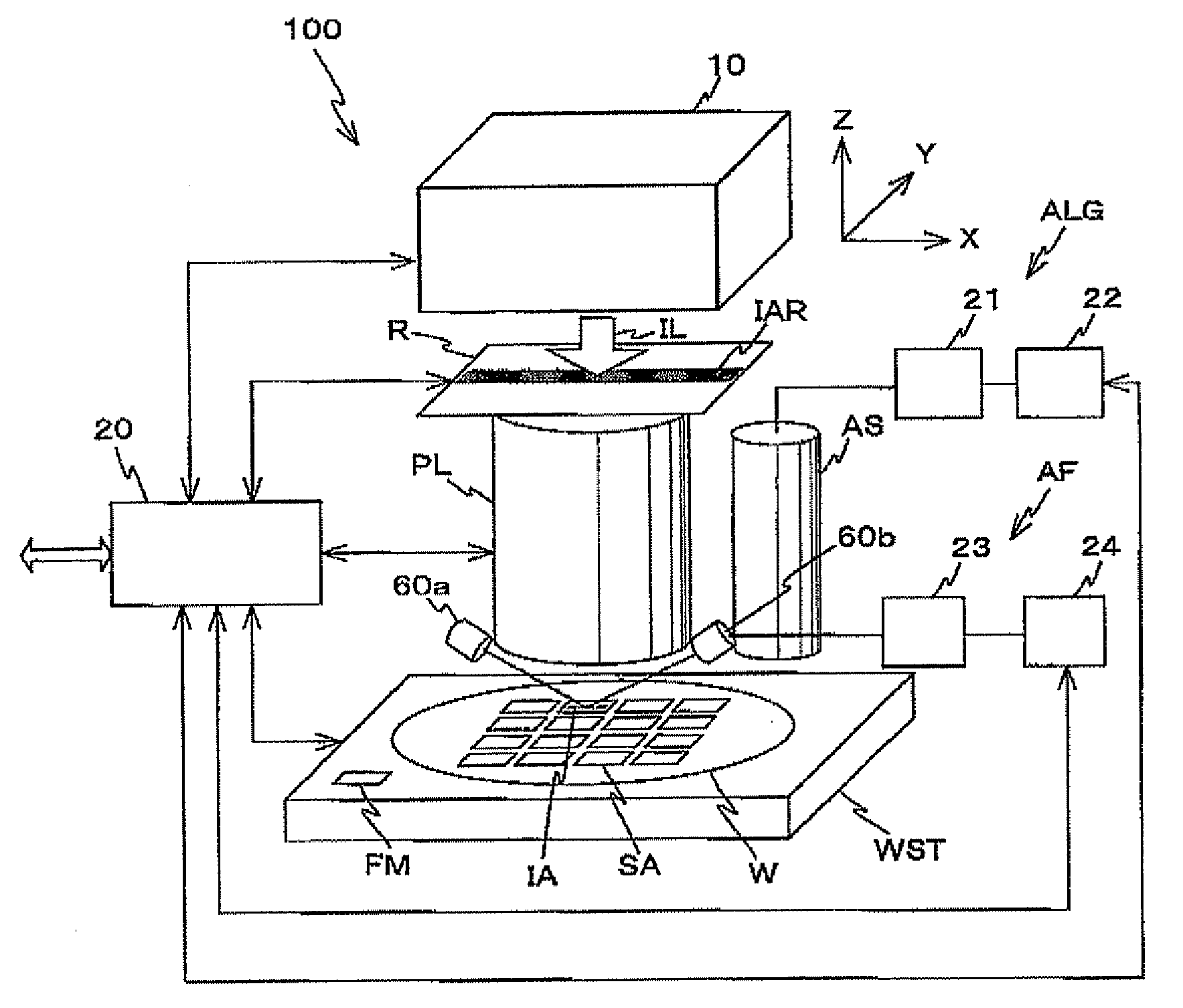
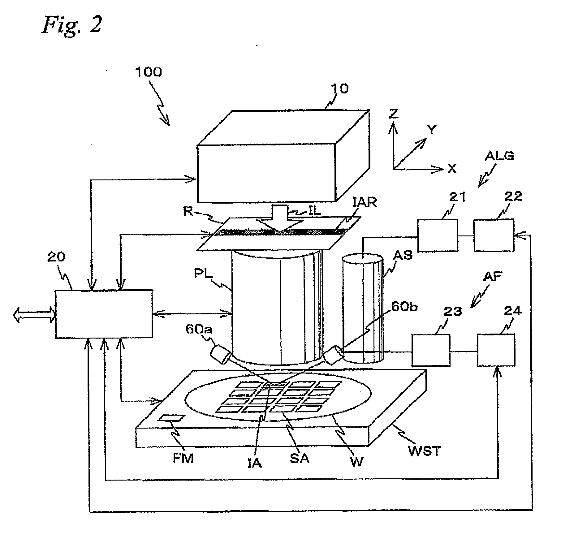
[0024]An embodiment of the present invention will be described below, referring to FIGS. 1 to 6.

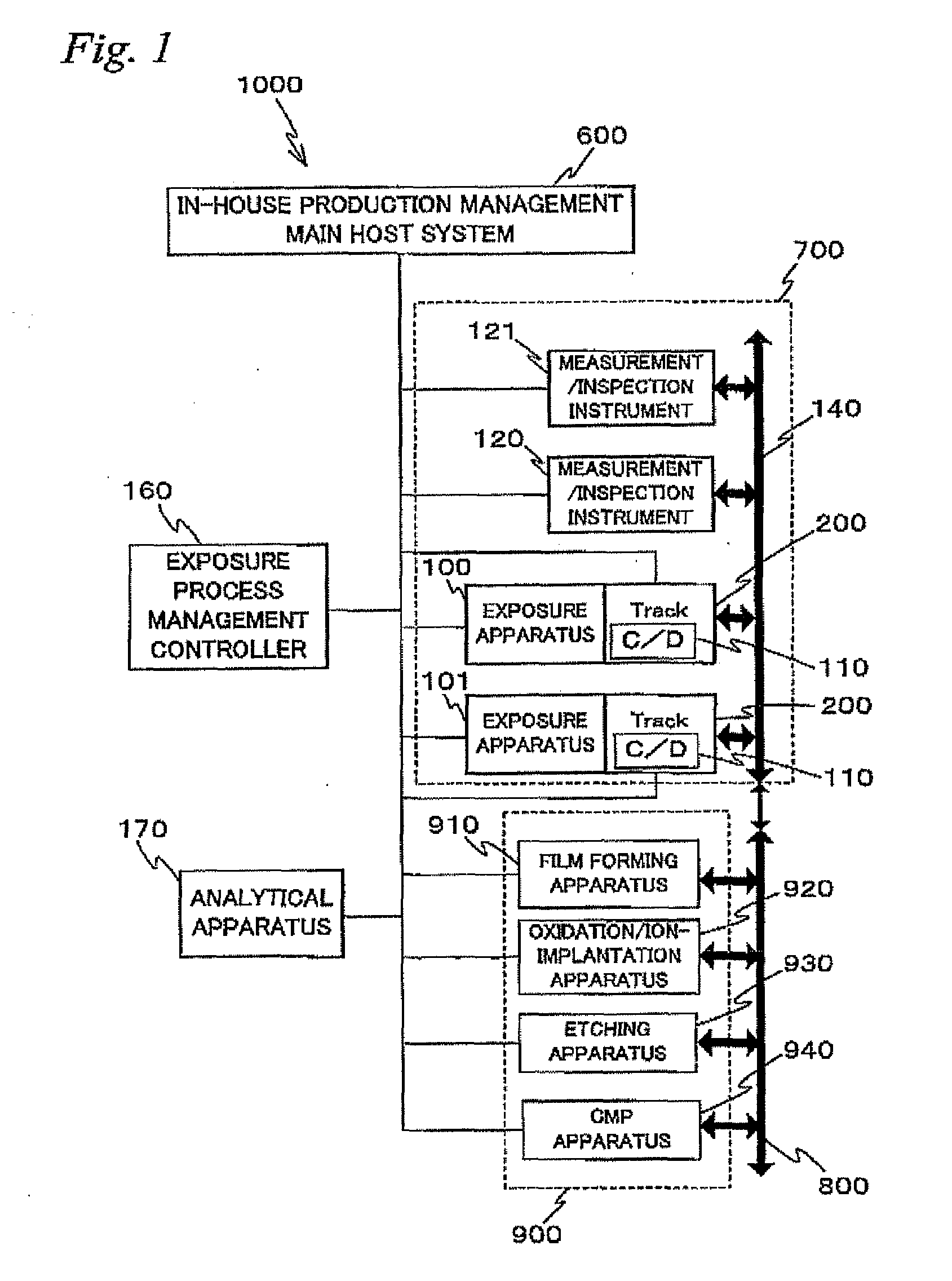
[0025]FIG. 1 shows a schematic configuration of a device manufacturing / processing system 1000 related to the embodiment. As shown in FIG. 1, device manufacturing / processing system 1000 is equipped with an in-house production management main host system 600, an exposure cell 700, a carrier line 800, a device manufacturing / processing apparatus group 900, an exposure process management controller (hereinafter, shortly referred to as a “management controller”) 160, and an analytical apparatus 170.

[In-House Production Management Main Host System]

[0026]In-house production management main host system (hereinafter, referred to as “host”) 600 is a main host computer that grasps the state of the entire device manufacturing / processing system 1000, and performs overall control of exposure cell 700, carrier line 800, device manufacturing / processing apparatus group 900, management controller 160, and a...


PUM

PropertyMeasurementUnit
pattern defect inspectionaaaaaaaaaa
frequencyaaaaaaaaaa
defect inspectionaaaaaaaaaa

Abstract

In the case where measurement/inspection of a wafer is performed in a measurement/inspection instrument before and after exposure is performed in an exposure apparatus, various kinds of conditions of the exposure apparatus and the measurement/inspection instrument such as environment in the apparatus/instrument, a measurement condition of an alignment system a measurement condition of an AF measurement device, a wafer grid, and image distortion are made to be matched. In particular, in accordance with a processing state of the exposure apparatus and a coater developer, a measurement result of a film, and the like, exclusion of a mark for overlay error measurement, adjustment of the measurement condition and correction of the measurement result, adjustment of the environment, correction of the measurement result according to the environment, and adjustment of pattern defect inspection are performed. Further, in calibration processing, aberration of a projection optical system of an exposure apparatus that transfers a pattern on a wafer for calibration, and the like are also taken into consideration. Accordingly, the yield of device production can be improved.

Description

CROSS-REFERENCE TO RELATE APPLICATIONS[0001]This application is a continuation of International Application PCT / JP2007 / 054279, with an international filing date of Mar. 6, 2007, the disclosure of which is hereby incorporated herein by reference in its entirety, which was not published in English.BACKGROUND OF THE INVENTION[0002]1. Field of the Invention[0003]The present invention relates to device manufacturing methods, device manufacturing systems, and measurement / inspection apparatuses, and more particularly, to a device manufacturing method including a lithography process, for example, for manufacturing semiconductor devices, liquid crystal display devices, imaging devices such as CCD (charge-Coupled Device), thin film magnetic heads and the like, a device manufacturing system, and a measurement / inspection apparatus.[0004]2. Description of the Background Art[0005]A device such as a semiconductor device is manufactured by repeating a series of a plurality of substrate processing s...

Claims


Application Information

Patent Timeline
Patent Type & Authority Applications(United States)
IPC IPC(8): G03B27/42G03B27/32G01N37/00
CPCG03F7/70516G03F7/70616G03F7/7085H01L22/20H01L2924/0002H01L2924/00G03F7/705G03F7/7065
Inventor OKITA, SHINICHIYASUKAWA, KOJI
Owner NIKON CORP
Why Eureka
Try Eureka