Substrate Joining Member and Three-Dimensional Structure Using the Same

a three-dimensional structure and joining member technology, applied in the direction of electrical equipment construction details, manufacturing tools, soldering apparatus, etc., can solve the problems of insufficient modification insufficient stress reduction of the connecting lead-wire terminal, and large connection section of the pin connector, so as to maintain reliability, increase shock resistance, and reduce the effect of impa

Inactive Publication Date: 2009-01-08
PANASONIC CORP
View PDF5 Cites 23 Cited by
  • Summary
  • Abstract
  • Description
  • Claims
  • Application Information

AI Technical Summary

Benefits of technology

[0015]The present invention addresses the problems discussed above, and aims to provide a substrate joining member capable of connection with a fine pitch and maintaining reliability at its connecting section when stress such as drop impact is applied to the substrate joining member. The present invention also provides a three-dimensional structure using the same substrate joining member.
[0016]The substrate joining member of the present invention includes a plurality of lead terminals made of electrically conductive material and an insulating housing to which the multiple lead terminals are fixed in a predetermined array. Each one of the lead terminals includes an upper end connecting section at a top face of the housing and a lower end connecting section at an underside of the housing. The housing includes a projection on at least two faces of its outer wall. This structure allows a three-dimensional structure connected with this substrate joining member to bear large impact because two boards and the substrate joining member unified into one body as a whole receive the impact. The three-dimensional structure is thus free from locally focused stress, so that it increases shock resistance. As a result, the three-dimensional structure excellent in shock resistance is obtainable although it employs fine-pitch connection.

Problems solved by technology

However, the foregoing connecting structure tends to subject a connected section of the pin connector to great force when a change in temperature causes the members forming this connected section to change differently in dimensions or when this connected section receives external impact.
This structure, however; uses both sides of the module board inefficiently, and the presence of through holes constrains the board from increasing a density of the circuit pattern.
The market expects that a circuit pattern be of a higher density and a lead shape be smaller, so that simple tricks such as a modification of a connecting lead-wire terminal are not enough to dampen the stress.

Method used


Image

  • Substrate Joining Member and Three-Dimensional Structure Using the Same
  • Substrate Joining Member and Three-Dimensional Structure Using the Same
  • Substrate Joining Member and Three-Dimensional Structure Using the Same

Examples


embodiment 1

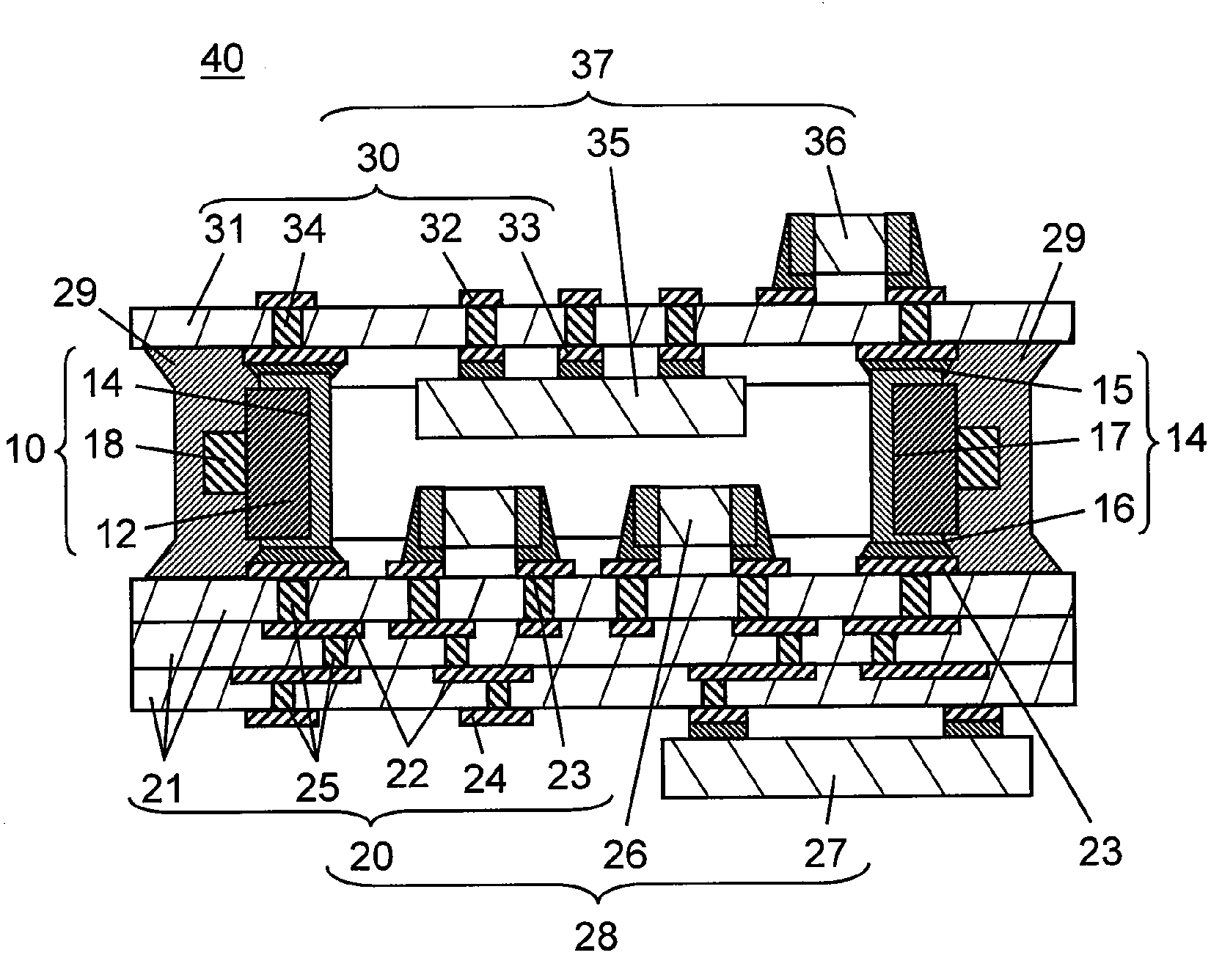
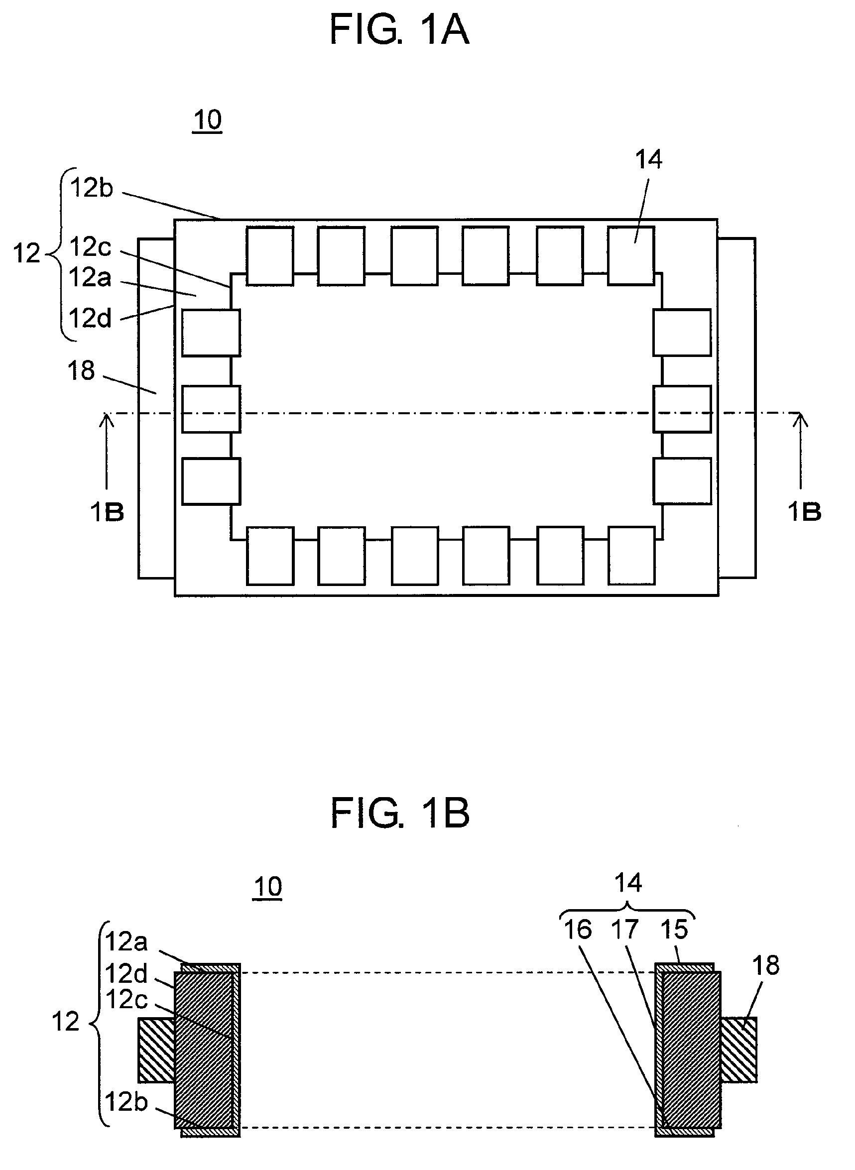
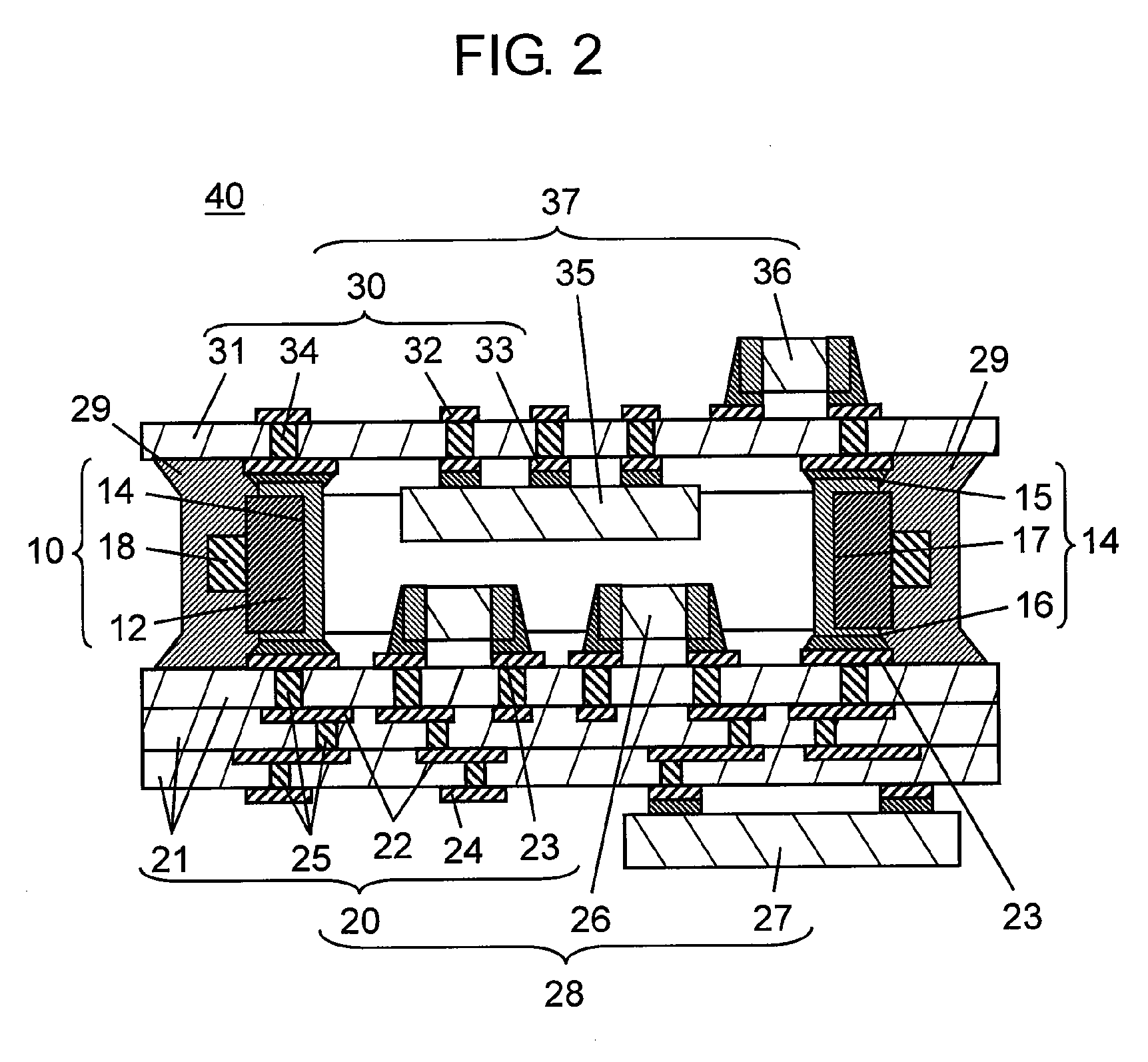
[0070]FIG. 1A shows a top view of substrate joining member 10 in accordance with the first embodiment of the present invention, and FIG. 1B shows a schematic sectional view of substrate joining member 10 shown in FIG. 1A cut along line 1B-1B.

[0071]As shown in FIG. 1A, substrate joining member 10 includes a plurality of lead terminals 14 made of electrically conductive material such as metal sheet and frame-like insulating housing 12 to which multiple lead terminals 14 are fixed vertically in a predetermined array. As shown in FIG. 1B, each one of lead terminals 14 is formed of upper end connecting section 15 disposed on top face 12a of housing 12, lower end connecting section 16 disposed on underside 12b of housing 12, and lead connecting section 17 disposed on inner wall 12c.

[0072]Housing 12 includes projections 18 formed on at least two faces 12d of its outer wall of the frame-like housing 12. Housing 12 is made from resin such as liquid crystal polymer, polyphenylene sulfide, po...

embodiment 2

[0097]FIGS. 5 and 6 show sectional views of a three-dimensional structure in accordance with the second embodiment of the present invention. The second embodiment differs from the first embodiment in a shape of the projection of the substrate joining member. This modification of the projection allows the projection to be fit more firmly into the resin filled-in. Other structures remain the same as those in the first embodiment.

[0098]FIG. 5 shows a sectional view of three-dimensional structure 65, which employs substrate joining member 10 equipped with projections 62 on outer wall face 61. The cross section of projections 62 viewed from vertical direction with respect to top face 63 and underside 64 of housing 59 shows that each one of projections 62 tapers from its tip 66 toward outer wall face 61. First and second module boards 28, 37 are unified into one body with substrate joining member 10 and resin 29, so that tapering projection 62 allows reinforcing the fit between projection...

embodiment 3

[0101]FIGS. 7-9 show sectional views of three-dimensional structures in accordance with the third embodiment of the present invention. In this third embodiment, a hole is formed in a region between the housing and the projection, and the hole is filled with resin, so that the projection can be fit into the resin more firmly. Other structures remain unchanged from those in the first embodiment.

[0102]FIG. 7 shows a sectional view of three-dimensional structure 75, which includes through-hole 72 in region 71 between projection 73 and housing 59. Hole 72 is formed vertically with respect to top face 63 and underside 64 of substrate joining member 10. Substrate joining member 10 having the structure discussed above connects first module board 28 and second module board 37 together, and outer wall face 61 surrounds the connected unit. Resin 29 is filled into the space outside the outer wall face 61, and then though-hole 72 vertically formed in region 71 is also filled with resin 29. This ...


PUM

PropertyMeasurementUnit
stressaaaaaaaaaa
electrically conductiveaaaaaaaaaa
three-dimensional structureaaaaaaaaaa

Abstract

Three-dimensional structure (40) of the present invention includes first module board (28), second module board (37), and substrate joining member (10) that unifies board (28) and board (37) into one body, thereby electrically connecting these two elements together. The unification is done by molding the outer wall of housing (12) of substrate joining member (10) with resin (29). Substrate joining member (10) used in the three-dimensional structure (40) includes multiple lead terminals (14) made of conductive material, and a frame-shaped and insulating housing (12) to which frame the lead terminals (14) are fixed vertically in a predetermined array. Housing (12) includes projections (18) on at least two outer wall faces of its frame shape.

Description

TECHNICAL FIELD[0001]The present invention relates to a substrate joining member for connecting multiple boards together, to which semiconductor elements (hereinafter referred to as IC chips) and chip components are mounted, and it also relates to a three-dimensional structure using the same substrate joining member.BACKGROUND ART[0002]Boards such as module boards, on which IC chips and chip components are mounted, have been conventionally connected to each other by a substrate joining member. The substrate joining member includes a multi-pole connector formed of a plug and a socket, or a pin connector formed of multiple connecting pins fixed to a spacer made of resin.[0003]Meanwhile mobile devices have been downsized, light-weighted and yet sophisticated, which increases the number of connecting terminals between module boards while a pitch between each one of the connecting terminals becomes narrower. The substrate joining member thus needs to be downsized so that an area per pin ...

Claims


Application Information

Patent Timeline
Patent Type & Authority Applications(United States)
IPC IPC(8): H05K1/14H01R12/00
CPCB23K1/0016B23K2201/42H05K1/144H05K2203/1572H05K2201/10378H05K2201/10977H05K2201/2018H05K3/368B23K2101/42
Inventor MORI, MASATOKOMYOJI, DAIDONAGAI, KOICHIYAGI, YOSHIHIKO
Owner PANASONIC CORP
Why Eureka
Try Eureka