
Synchronous semiconductor device and data processing system including the same

Active Publication Date: 2009-01-15
RAMBUS INC
View PDF5 Cites 9 Cited by
  • Summary
  • Abstract
  • Description
  • Claims
  • Application Information

AI Technical Summary

Benefits of technology

[0006]It is therefore an object of the present invention to provide an improved synchronous semiconductor device capable of reducing consumed power of an input circuit unit in response to a chip select signal being inactive.
[0007]Another object of the present invention is to provide a synchronous semiconductor device capable of reducing consumed power without stopping an operation of an input buffer or an internal clock signal, in response to a chip select signal being inactive.
[0008]Still another object of the present invention is to provide a synchronous semiconductor device capable of reducing consumed power generated between an input buffer and a latch circuit, in response to a chip select signal being inactive.
[0009]Still another object of the present invention is to provide a synchronous semiconductor device capable of reducing a charge / discharge current of a delay circuit used for a timing adjustment of an address signal, a command signal or the like in response to a chip select signal being inactive.
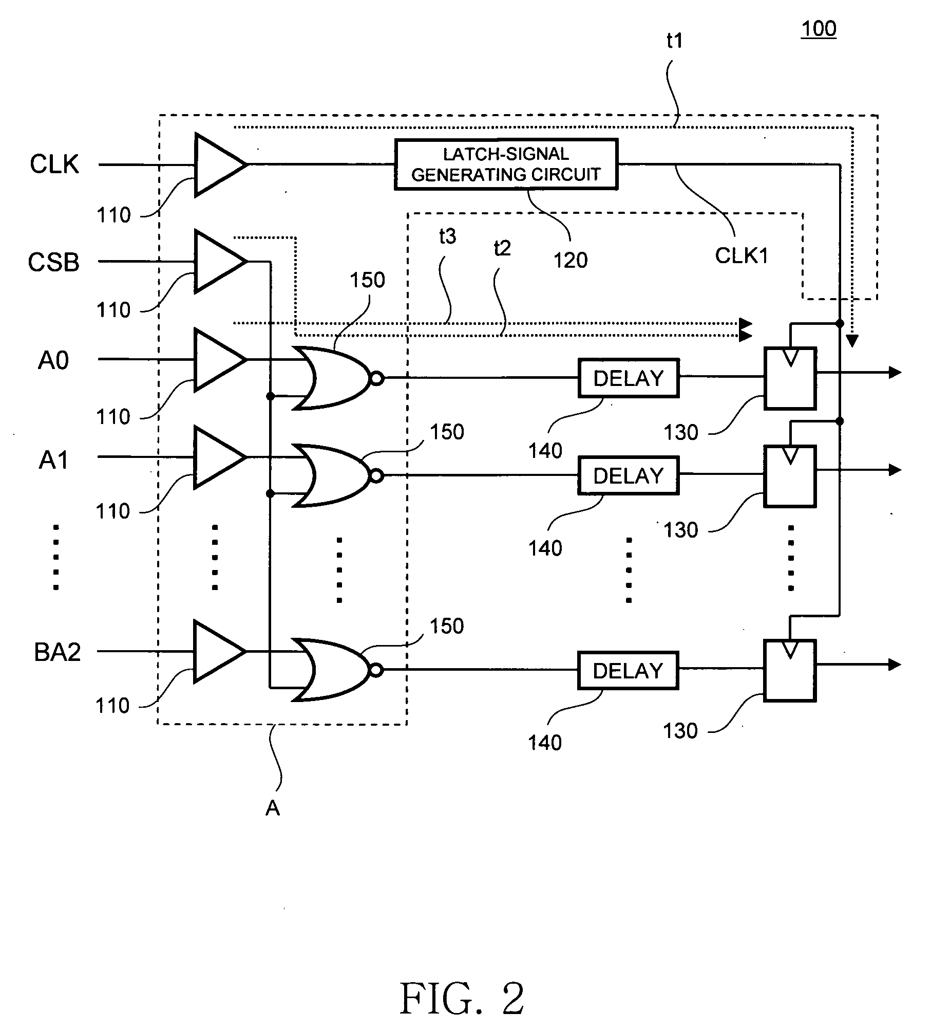
[0018]As described above, according to the present invention, a gate circuit that causes the internal input signal or a decode signal thereof to become inactive in response to a chip select signal becoming inactive is arranged at a previous stage of a delay circuit having a large charge / discharge current. Accordingly, without stopping an operation of an input buffer or an internal clock signal, consumed power generated between the input buffer and the latch circuit can be effectively reduced.

Problems solved by technology

However, when the bias current of the differential amplifier circuit is cut, a predetermined time is necessary to make the differential amplifier circuit operable again, and therefore, when the frequency of the clock signal is particularly high, adopting such a method is difficult.
However, when an internal clock signal is stopped, restoring the internal circuit takes time, and therefore, it is thought to be inappropriate to stop the clock signal itself in sequence with the chip select signal.
Therefore, even when an operation of the latch circuit is stopped, a charge / discharge current generated from an operation of the delay circuit or the like cannot be reduced.

Method used


Image

  • Synchronous semiconductor device and data processing system including the same
  • Synchronous semiconductor device and data processing system including the same
  • Synchronous semiconductor device and data processing system including the same

Examples


Embodiment Construction

[0028]Preferred embodiments of the present invention will now be explained in detail with reference to the drawings.

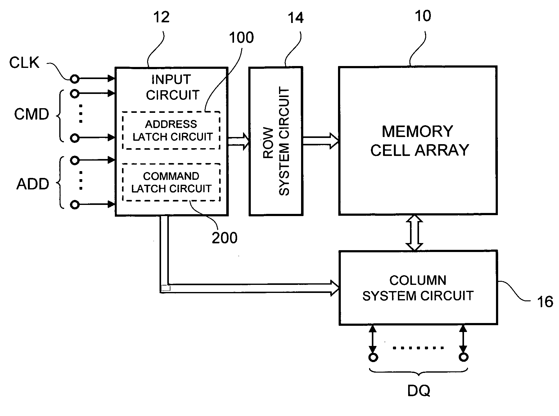
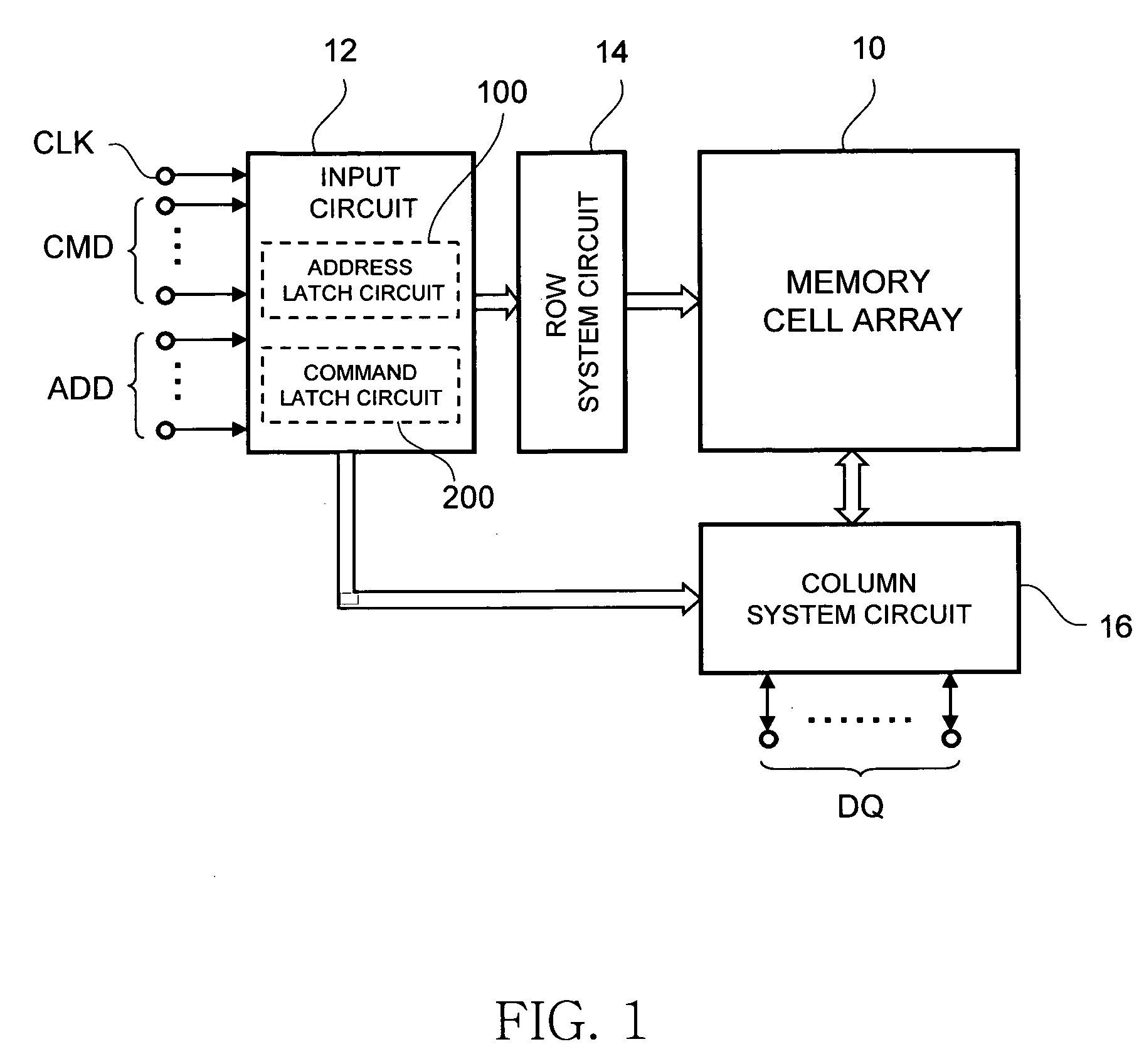
[0029]FIG. 1 is a block diagram showing a configuration of a synchronous semiconductor device according to a preferred embodiment of the present invention.

[0030]The synchronous semiconductor device according to the present embodiment is a synchronous DRAM, and includes a memory cell array 10, an input circuit 12 that receives various external input signals, and a row system circuit 14 and a column system circuit 16, each of the circuits which executes a row system access for the memory cell array 10 and a column system access therefor, as shown in FIG. 1.

[0031]When reading data from the memory cell array 10, a read command is issued via a command terminal CMD, and an address signal to be read is supplied via an address terminal ADD. Thereby, the data read from the memory cell array 10 is outputted via a data input / output terminal DQ. On the other hand, when writing dat...


PUM


Abstract

A synchronous semiconductor device includes: input buffers; a latch-signal generating circuit that generates a latch signal based on a clock signal; latch circuits that latch an address signal in response to the latch signal; delay circuits that supply the latch circuits with the address signal in synchronism with the latch signal; NOR gate circuits that inactivate the address signal in response to a chip select signal becoming inactive, the NOR gate circuits being arranged between the input buffers and the delay circuits. According to the present invention, without stopping an operation of the input buffers or an internal clock signal, consumed power generated between the input buffers and the latch circuits can be effectively reduced.

Description

TECHNICAL FIELD[0001]The present invention relates to a synchronous semiconductor device that operates in synchronism with a clock signal, and, more particularly relates to an input circuit that fetches an address signal or a command signal. The present invention also relates to a data processing system having such a synchronous semiconductor device.BACKGROUND OF THE INVENTION[0002]Most of semiconductor devices such as a DRAM (Dynamic Random Access Memory) or the like are of a type which operates in synchronism with a clock signal. In such a synchronous semiconductor device, when a frequency of the clock signal rises, consumed power of an input circuit that fetches an address signal or a command signal increases, and therefore various kinds of propositions for reducing the consumed power of the input circuit at a time of being inactive have been made (see Japanese Patent Application Laid-open Nos. H7-230688, H11-16349, and 2007-12128).[0003]For example, Japanese Patent Application L...

Claims


Application Information

Patent Timeline
IPC IPC(8): G11C7/00G11C8/00
CPCG11C7/1072G11C7/1078G11C7/109G11C11/4093G11C7/222G11C8/18G11C11/4076G11C7/22
Inventor KINOSHITA, HIROTOFUJISAWA, HIROKI
Owner RAMBUS INC
Learn More