
Multi-information-layer recording medium and manufacturing process

Inactive Publication Date: 2009-01-15
HITACHI LTD
View PDF5 Cites 4 Cited by
  • Summary
  • Abstract
  • Description
  • Claims
  • Application Information

AI Technical Summary

Benefits of technology

[0012]Problems which arise when the thin space layers are formed are a plate thickness distribution, warp, burr, and the like attributable to a polycarbonate substrate that is inject-molded by an injection. In a plastic injection molding in which no surface polishing is performed, it is extremely difficult to suppress plate thickness unevenness to several nm, thus causing unevenness of at least several μm. Likewise, regarding the warp and burr, it is difficult to require accuracy equivalent to that of, for example, Si wafer. In the case of performing pattern transfer using this type of substrate, when a flat and hard stamper, serving as a mother mold, is used, a space layer, which is formed so as to be sandwiched between the substrate and the stamper, is affected by plate thickness distribution, warp, burr attributable to the substrate itself, thus causing unevenness of spacer thickness. When the stamper is warped, thickness unevenness is caused in the space layer by influences of both the stamper and the substrate. In the case of forming a thick space layer, these influences attributable to the polycarbonate substrate exerted on the space layer was small, and therefore no problem was caused. Moreover, in the case of a DVD two-layer disc having a space layer in average thickness of 55 μm, an allowable range of thickness unevenness was large enough such as 45 μm to 65 μm, and therefore no problem was caused in this point.
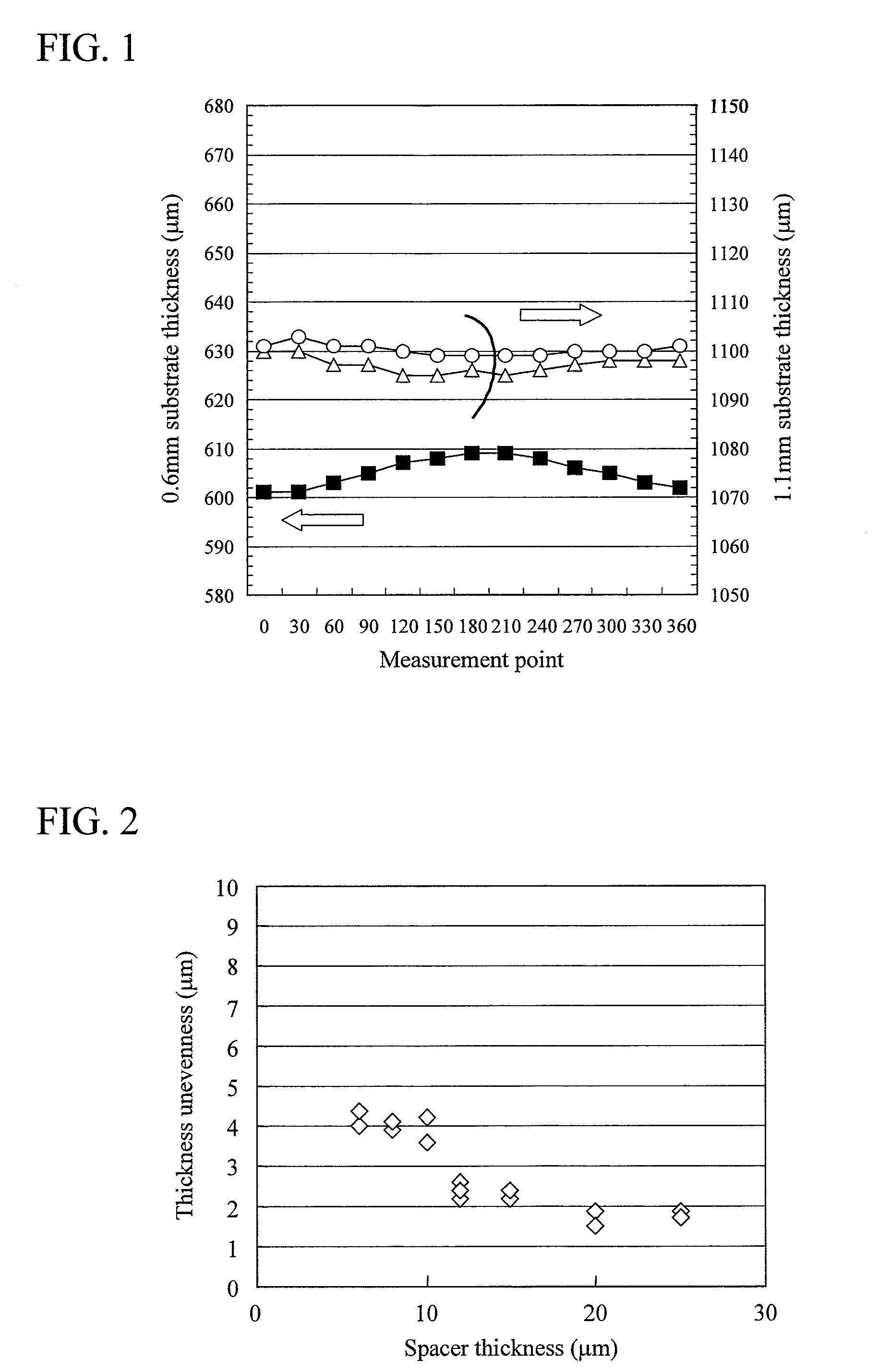
[0026]According to the present invention, it is possible to obtain a multi-information-layer recording medium wherein a space layer having thickness unevenness of 2 μm or less is formed even in a space layer having a thickness of 15 μm or less to thereby provide a stable interlayer switching and an excellent characteristic.

Problems solved by technology

Moreover, when the number of layers is increased by forming a multilayer, an allowable range of thickness unevenness per layer becomes more severe with an increase in the number of layers.
Likewise, in the case of four layers, an allowable range of thickness unevenness per layer is 2 μm, in the case of five layers, an allowable range of thickness unevenness per layer is 1.6 μm, in the case of six layers, an allowable range of thickness unevenness per layer is 1.33 μm, and in the case of eight layers, an allowable range of thickness unevenness per layer is 1 μm, and therefore it is difficult to manufacture the thin space layer evenly and accurately.
Though the average thickness of space layers with respect to the number of layers and design of the cover layer are different depending on the differences in spherical aberration correction amount and device performance, forming thin space layers evenly still remains difficult.
Problems which arise when the thin space layers are formed are a plate thickness distribution, warp, burr, and the like attributable to a polycarbonate substrate that is inject-molded by an injection.
In a plastic injection molding in which no surface polishing is performed, it is extremely difficult to suppress plate thickness unevenness to several nm, thus causing unevenness of at least several μm.
Likewise, regarding the warp and burr, it is difficult to require accuracy equivalent to that of, for example, Si wafer.
In the case of performing pattern transfer using this type of substrate, when a flat and hard stamper, serving as a mother mold, is used, a space layer, which is formed so as to be sandwiched between the substrate and the stamper, is affected by plate thickness distribution, warp, burr attributable to the substrate itself, thus causing unevenness of spacer thickness.
When the stamper is warped, thickness unevenness is caused in the space layer by influences of both the stamper and the substrate.
Simply judging from the result, a maximum gap is 17 μm between the substrate having a thickness of 1.1 mm and the substrate having a thickness of 0.6 mm which is obtained by combining them (either one of them is used as a stamper), and when a space layer is formed using this gap, this results in unevenness of spacer thickness.
Even when a Ni stamper having a flat plate thickness is used, unevenness of plate thickness of one substrate remains, and by this influence, unevenness of spacer thickness is caused.

Method used


Image

  • Multi-information-layer recording medium and manufacturing process
  • Multi-information-layer recording medium and manufacturing process
  • Multi-information-layer recording medium and manufacturing process

Examples


Embodiment Construction

[0045]The following will explain an embodiment of the present invention with reference to the drawings.

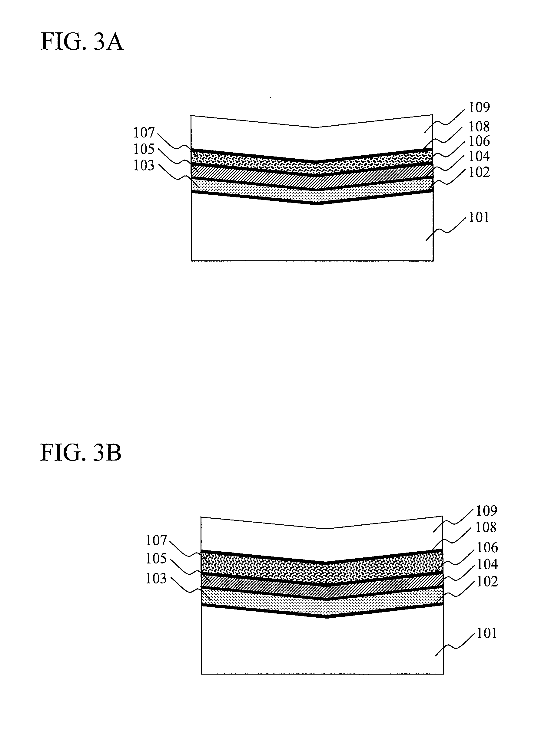
[0046]FIG. 3A and FIG. 3B show part of a cross-sectional structure of a manufactured multi-information-layer recording medium, respectively. The structure is formed including four information layers 102, 104, 106 and 108 on a substrate 101 with a cover layer 109 being formed thereon. Translucency spacers 103, 105, 107 are respectively sandwiched in between the information layers 102, 104, 106, and 108. FIG. 3A shows a structure where the thickness of each spacer is substantially the same one another and FIG. 3B shows a structure where the thickness of each spacer is different from one another.

[0047]FIGS. 4A to 4I, and FIG. 5 show a manufacturing process and a manufacturing flow, respectively. The manufacturing process to be explained here is applicable to not only a medium where the thickness of each spacer is substantially the same one another shown in FIG. 3A but also a medium wh...


PUM

PropertyMeasurementUnit
Lengthaaaaaaaaaa
Lengthaaaaaaaaaa
Thicknessaaaaaaaaaa

Abstract

In forming a space layer of a multi-formation-layer recording medium, there are provided a medium having a high precision in a thickness of the space layer and its manufacturing process. In the multi-formation-layer recording medium wherein at least two pairs of an information recording layer and a translucency spacer are layered on a substrate having physical patterns composed of an optical spot groove and / or pits on the surface, an average thickness of the translucency spacers in an information zone is 15 μm or less, and a difference in spacer thickness between a minimum value and a maximum value is 2 μm or less.

Description

CLAIM OF PRIORITY[0001]The present application claims priority from Japanese patent application JP 2007-182008 filed on Jul. 11, 2007, the content of which is hereby incorporated by reference into this application.BACKGROUND OF THE INVENTION[0002]1. Field of the Invention[0003]The present invention relates to a multi-information-layer recoding medium having a plurality of information layers and its manufacturing process.[0004]2. Description of the Related Art[0005]The following will explain the conventional method for manufacturing an optical disc substrate. A plastic substrate material such as polycarbonate melt at high temperature is injected, with a high pressure, into a mold with a metal stamper placed therein, and thereafter the resultant is cooled and taken out. Then a plastic substrate having physical patterns copied on its surface is completed. This injection molding method (injection method) is one that is generally used in manufacturing plastic substrates for the currently...

Claims


Application Information

Patent Timeline
IPC IPC(8): B32B3/28G11B7/24G11B7/24038G11B7/2533G11B7/254G11B7/257
CPCG11B7/24038Y10T428/21G11B7/263
Inventor ANZAI, YUMIKOUSHIYAMA, JUNKOSHINTANI, TOSHIMICHI
Owner HITACHI LTD
Learn More