High performance mixed signal circuit

a mixed signal and high-performance technology, applied in the field of mixed signal circuits, can solve the problems of extremely high signal fidelity, data-dependent digital activity and temperature variations, and inducing temperature variations and other deleterious effects in analog circuitry, and achieve the effect of reducing the data dependency of toggle activity

Active Publication Date: 2009-01-22
KEYSIGHT TECH
View PDF2 Cites 1 Cited by
  • Summary
  • Abstract
  • Description
  • Claims
  • Application Information

AI Technical Summary

Benefits of technology

[0030]In a second aspect the invention relates to a method for reducing data dependency of toggle activity in a mixed signal circuit comprising a first circuit for direct digital synthesis. The method comprises the steps of applying a randomised signal to a phase generator of the first circuit for direct digital synthesis by combining the initial phase generator input signal with a pseudo-random noise signal and by feeding the pseudo-random noise signal to a second circuit for direct digital synthesis such that perturbation caused by applying the randomised signal to the first circuit is compensated for.

Problems solved by technology

This current surge, together with power supply parasitics causes ringing on Vdd and Vss lines.
In data converters (DAC, ADC) with on-chip digital signal processing, there is also a concern regarding data-dependent power dissipation in the digital portions that can induce temperature variations and other deleterious effects in the analog circuitry.
In signal source applications, the generation of a carrier wave (CW) signal often requires extremely high signal fidelity, so the carrier wave application is very sensitive to the abovementioned spurious mechanisms.
There is a major challenge to reduce the data-dependent digital activity and temperature variations with an acceptable cost in digital resources.

Method used


Image

  • High performance mixed signal circuit
  • High performance mixed signal circuit
  • High performance mixed signal circuit

Examples


Embodiment Construction

[0035]The present invention proposes digital circuitry wherein the detrimental effects of spurious signals in associated mixed-signal circuitry are drastically reduced. The proposed design displays an improved performance by achieving the following assets:[0036]reducing the data dependency of toggle activity, and[0037]equalizing the digital activity over time

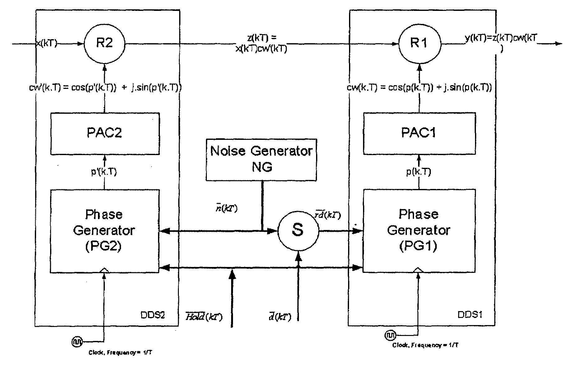
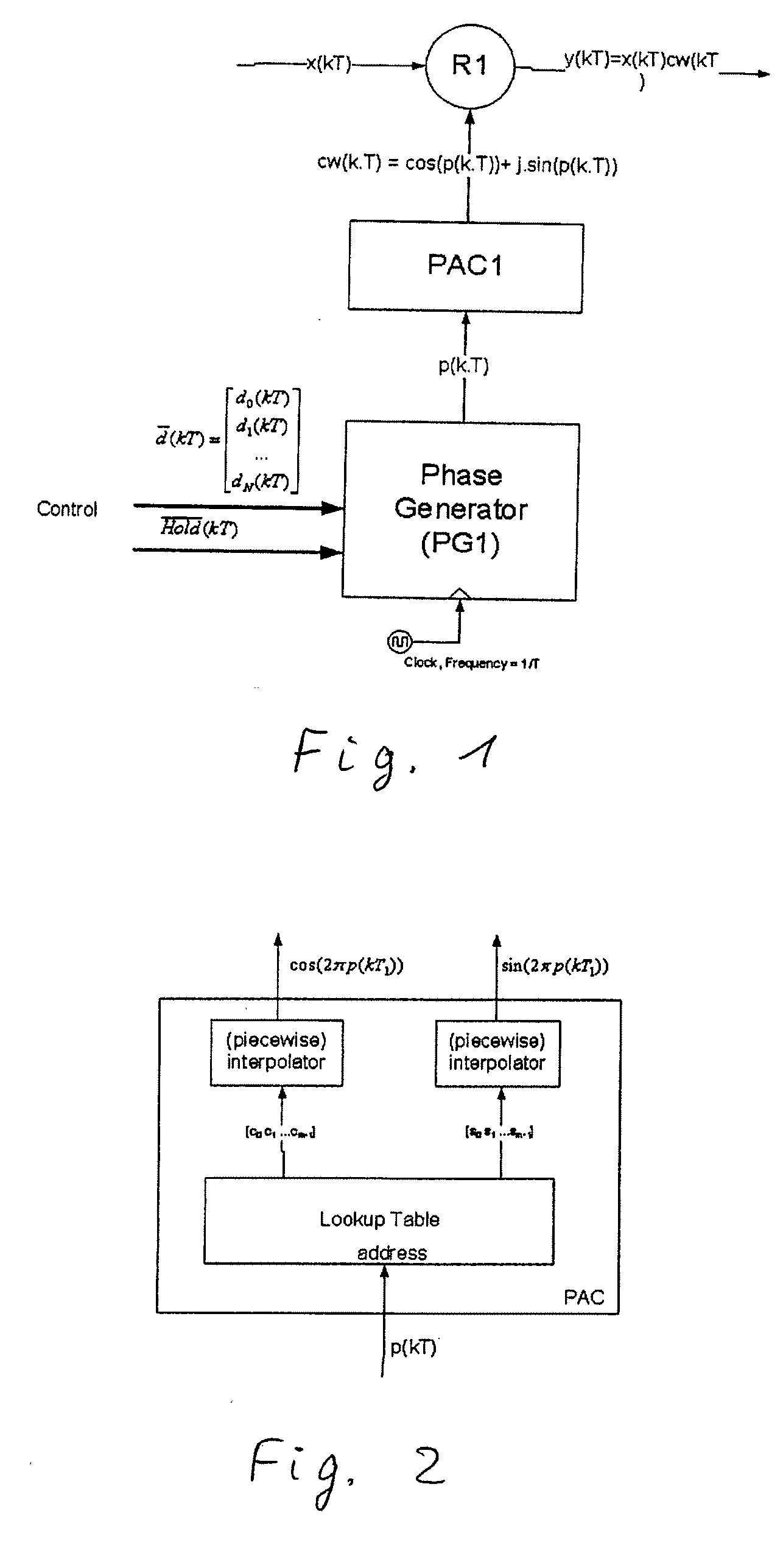
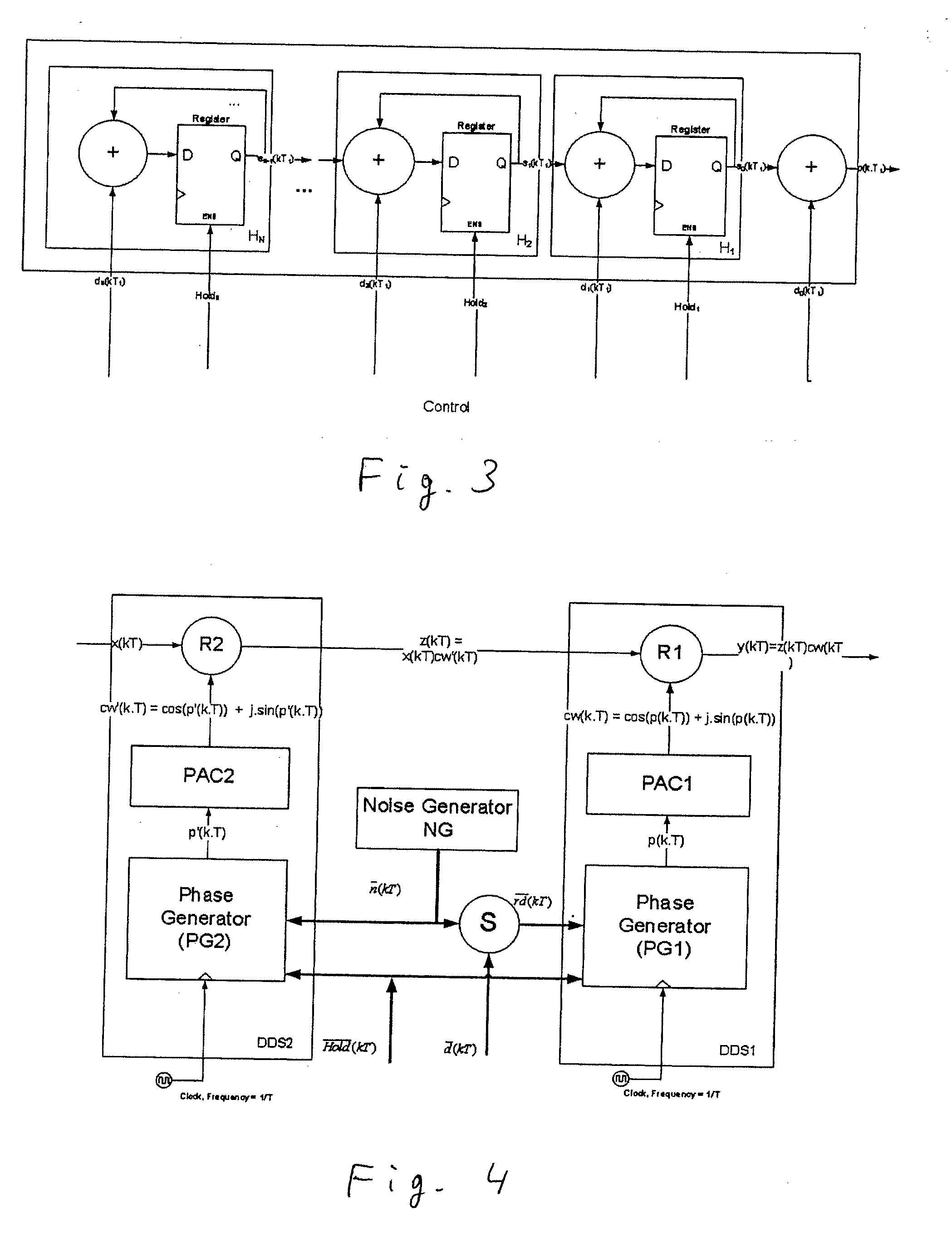
[0038]FIG. 4 shows a DDS based modulator circuit which allows reducing the data dependency of the toggle activity. The DDS1 circuitry, comprising R1, PAC1 and PG1, is exactly the same as in the original circuit in FIG. 1.

[0039]The Noise Generator (NG) generates a vector signal n(kT)=[n0(kT) n1(kT) . . . nN(kT)]T. Generally this signal would be provided by a long PN generator to make it noise-like.

The Subtractor (S) (or alternatively an adder) is a vector operator that perturbates the input signal d(kT) with n(kT) into a randomized vector signal rd(kT)= d(kT)−n(kT), which is then applied to the DDS circuitry. This disconnects the...


PUM


Abstract

The present invention is related to a digital circuit for use in a mixed-signal circuit. The digital circuit comprises:a first circuit for direct digital synthesis comprising a first phase generator (PG1) arranged for being fed with a phase generator input signal, a first phase-to-amplitude converter (PAC1) arranged for being fed with a phase from the first phase generator and for generating a first carrier wave output, and first signal combining means (R1) for combining the first carrier wave output with a first input signal,a noise generator (NG) arranged for generating a pseudo-random noise signal,combining means (S) for combining the pseudo-random noise signal and the phase generator input signal such that the phase generator input signal to the first phase generator (PG1) is randomised,a second circuit for direct digital synthesis comprising a second phase generator (PG2) arranged for being fed with the pseudo-random noise signal, a second phase-to-amplitude converter (PAC2) arranged for being fed with a phase from the second phase generator and for generating a second carrier wave output, and second signal combining means (R2) for combining the second carrier wave output with a second input signal, whereby the second carrier wave output combined with the second input signal is comprised in the first input signal.

Description

FIELD OF THE INVENTION[0001]The present invention relates to a mixed-signal circuit wherein direct digital synthesis is applied.STATE OF THE ART[0002]In a mixed-signal environment state transitions in digital circuitry are an important origin for spurious components that are injected into analog circuitry.[0003]This is true, especially in mixed-signal integrated circuits (ICs) where the substrate constitutes a transmission path between the digital and analog circuitry.[0004]There are various mechanisms through which spurious signals are injected:[0005]during digital transitions (1->0 and 0->1), both NMOS and PMOS transistors conduct and a current flows from Vdd to Vss. This current surge, together with power supply parasitics causes ringing on Vdd and Vss lines. Bounces on Vdd and Vss lines are injected into the substrate.[0006]capacitive coupling via drain regions[0007]impact ionizationThese mechanisms occur for every switching gate.[0008]In data converters (DAC, ADC) with on...

Claims


Application Information

Patent Timeline
Patent Type & Authority Applications(United States)
IPC IPC(8): H03B21/00
CPCH04L27/2053G06F1/0342G06F1/022H04L27/00
Inventor VAN DE SANDE, FRANK
Owner KEYSIGHT TECH
Why Eureka
Try Eureka