

High-speed optical transceiver for infiniband and ethernet
- Summary
- Abstract
- Description
- Claims
- Application Information
AI Technical Summary
Benefits of technology
Problems solved by technology
Method used
Image

Examples
Embodiment Construction
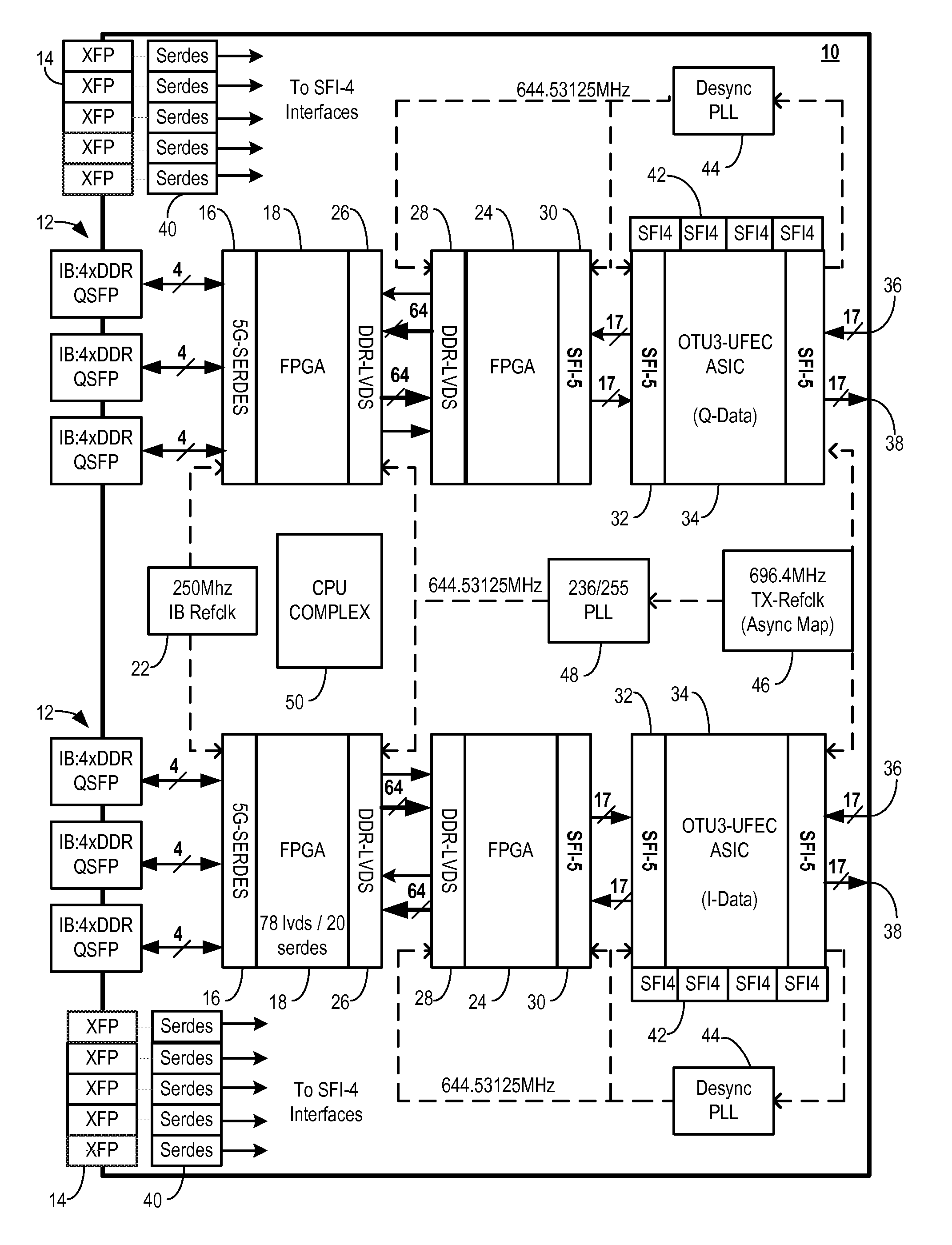
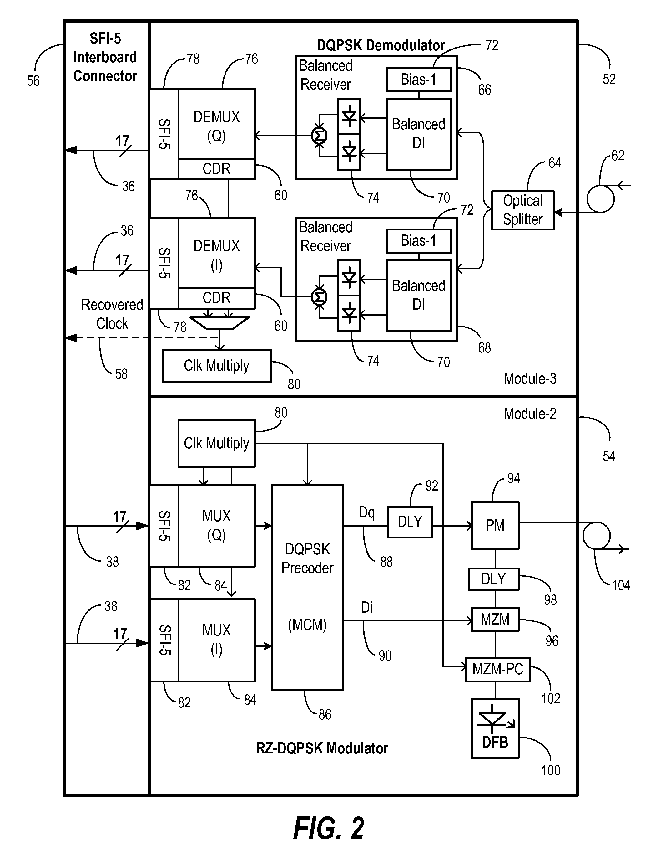
[0017]In various exemplary embodiments, the present invention provides a high-speed 100G optical transceiver for InfiniBand and Ethernet to frame InfiniBand (IB) and Ethernet into transparent Generic Framing Protocol (GFP-T). The optical transceiver utilizes an architecture which relies on standards-compliant (i.e., multi-sourced) physical client interfaces. These client interfaces are back-ended with flexible, programmable Field Programmable Gate Array (FPGA) modules to accomplish either IB or Ethernet protocol control, processing, re-framing, and the like. Next, signals are encoded with Forward Error Correction (FEC) and can include additional Optical Transport Unit (OTU) compliant framing structures. The resulting data is processed appropriately for the subsequent optical re-transmission, such as, for example, with differential encoding, Gray encoding, I / Q Quadrature encoding, and the like. The data is sent to an optical transmitter block and modulated onto an optical carrier. Al...
PUM
 Abstract
Description
Claims
Application Information