Printed wiring board

a wiring board and printed technology, applied in the direction of waveguides, waveguide type devices, high frequency circuit adaptations, etc., can solve the problems of wasting electric power, difficult to design the characteristic impedance of flexible wiring boards, and affecting the operation of flexible wiring boards

Inactive Publication Date: 2009-01-29
KK TOSHIBA
View PDF3 Cites 20 Cited by
  • Summary
  • Abstract
  • Description
  • Claims
  • Application Information

AI Technical Summary

Benefits of technology

[0012]It is an object of the present invention, in view of the above-described problems, to provide a printed-wiring board which can conduct the control of the characteristic impedance independent of the number of conductive pattern composing the printed-wiring board.
[0014]According to the aspect of the present invention, the electric power layer of the printed wiring board includes the mechanism for controlling the characteristic impedance of the printed wiring board. Therefore, the characteristic impedance of the printed wiring board can be easily controlled only by operating the mechanism even though the width of the wiring pattern is not controlled as in the past. As a result, the design of the wiring pattern in view of the current rating is not required so that the degree of freedom in design of the wiring pattern can be developed. For example, there is no advantage that the current rating of the wiring pattern, that is, the printed wiring board is increased even though the width of the wiring pattern is decreased in view of impedance matching.
[0016]In the embodiment, it is desired that the center of the wiring pattern in the width direction thereof is matched with the center of the trench in the width direction thereof. In this case, the characteristic impedance of the printed wiring board can be controlled effectively and absolutely by adjusting the width of the trench.
[0017]The aspects of the present invention as described above can be applied for any printed wiring board. However, the aspects can be applied more effectively and absolutely for a flexible printed wiring board by making the board of heat resistance resin base.
[0019]The flexible printed wiring board and the double-sided printed wiring board include no multilayered conductive pattern. As disclosed in Reference 1, therefore, if the multilayered conductive pattern is formed so that the conductive pattern located below the MSL (wiring pattern) is partially removed and the conductive pattern can not be superimposed with the MSL, the manufacturing cost of the printed wiring board is increased and the flexibility of the printed wiring board is reduced because the printed wiring board includes the multilayered conductive pattern. On the other hand, according to the aspects of the present invention, the characteristic impedance of the printed wiring board can be effectively controlled.
[0023]According to the aspect of the present invention can be provided a printed-wiring board which can conduct the control of the characteristic impedance independent of the number of conductive pattern composing the printed-wiring board.

Problems solved by technology

However, a flexible wiring board with large degree of freedom in structure is being employed as the electronic device is downsized.
Since the thickness of the flexible wiring board is small so as to realize the flexibility thereof, it is difficult to design the characteristic impedance of the flexible wiring board.
On the other hand, in this case, since the current rating of the flexible wiring board becomes small so that the wiring pattern of the flexible wiring board may be burned out.
In this case, however, since electric power consumption is increased as a whole and much current is consumed at the resistances, the electric power is wasted.
The technique disclosed in Reference 1, however, is effective for the multilayered wiring board with three or more, preferably, four or more conductive layers containing the MSL, but not effective for a flexible wiring board such as a double-sided printed wiring board which is configured such that the conductive patterns are formed on the main surface and the rear surface of the core board, respectively.

Method used


Image

  • Printed wiring board
  • Printed wiring board
  • Printed wiring board

Examples


Embodiment Construction

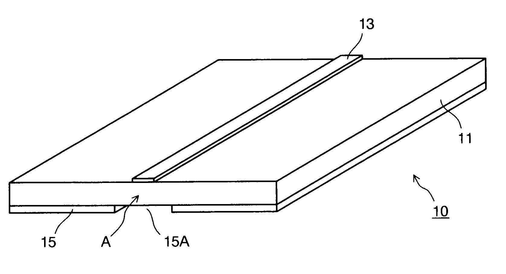
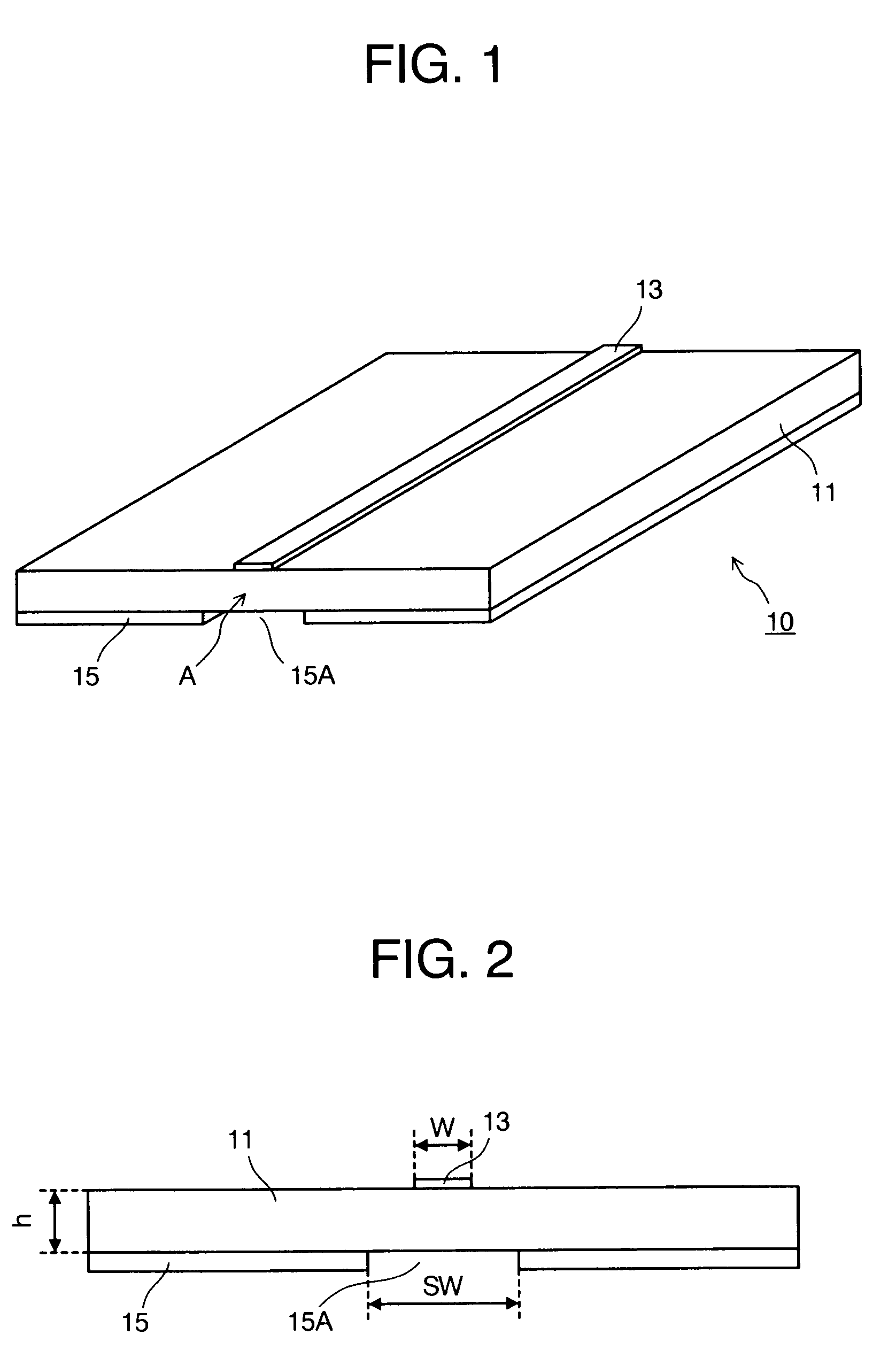
[0028]Hereinafter, the present invention will be described in detail with reference to the drawings. FIG. 1 is a perspective view illustrating an embodiment of the printed-wiring board according to the present invention. FIG. 2 is a side view of the printed-wiring board in FIG. 1, as viewed from the direction designated by the arrow “A”.

[0029]The printed-wiring board 10 illustrated in FIG. 1 includes aboard 11 made of insulator, a metallic conductor (wiring pattern) 13 to transfer (a) microwave electric signal(s) which is formed on the main surface of the board 11 and an electric power layer 15 formed on the rear surface of the board 11, thereby constituting a double-sided printed wiring board with a double-sided wiring structure. The electric power layer 15 is maintained a standard electric potential or shifted slightly from the standard electric potential so that the potential shift from the standard electric potential can be small enough to set the characteristic impedance of the...


PUM

PropertyMeasurementUnit
thicknessaaaaaaaaaa
thicknessaaaaaaaaaa
thicknessaaaaaaaaaa

Abstract

A printed wiring board includes a board made of insulator; a wiring pattern to transfer an electric signal which is made of patterned metallic conductor and formed on at least one of a main surface and a rear surface of the board; and an electric power layer formed on at least one of the main surface and the rear surface of the board; wherein the electric power layer includes a mechanism for controlling a characteristic impedance of the printed wiring board.

Description

CROSS-REFERENCE TO RELATED APPLICATIONS[0001]This application is based upon and claims the benefit of priority from the prior Japanese Patent Application No. 2007-194762, filed on Jul. 26, 2007; the entire contents of which are incorporated herein by reference.BACKGROUND OF THE INVENTION[0002]1. Field of the Invention[0003]The present invention relates to a printed-wiring board particularly requiring high speed operation, large current rating and flexibility.[0004]2. Description of the Related Art[0005]A printed wiring board, on which (an) IC chip(s) with high speed operationality is (are) mounted and which requires large current rating, is available for various electronic devices such as a computer, a magneto-optical memory and a cellular phone. With a conventional printed-wiring board, a high frequency signal is transferred under a transfer mode using a micro strip line (MSL), a strip line (SL) or a coplanar waveguide (CPW). In the conventional printed-wiring board, the thickness ...

Claims


Application Information

Patent Timeline
Patent Type & Authority Applications(United States)
IPC IPC(8): H05K1/00H01P3/08H01P3/14H05K3/00
CPCH01P3/003H01P3/08H05K1/0253Y10T29/49124H05K2201/09663H05K2201/0969H05K1/0393
Inventor SAITO, SHINICHIRO
Owner KK TOSHIBA
Why Eureka
Try Eureka