Organic light emitting display

a light-emitting display and organic technology, applied in the field of organic light-emitting displays, can solve the problems of increasing the threshold voltage of the drive transistor in the pixel circuit for flowing current, the brightness of the organic light-emitting display is gradually decreasing, and the current driving power is relatively low. the effect of reducing the threshold voltage change of the drive transistor and improving the overall brightness uniformity of the display

Active Publication Date: 2009-01-29
SEOUL NAT UNIV R&DB FOUND
View PDF3 Cites 40 Cited by
  • Summary
  • Abstract
  • Description
  • Claims
  • Application Information

AI Technical Summary

Benefits of technology

[0010]Accordingly, an object of the present invention is to provide an organic light emitting display that can minimize threshold voltage change of a drive transistor, in other words, degradation phenomenon and improve an overall brightness uniformity of the display by dividing an image display period of one frame into first and second periods, and applying a positive (or negative) voltage as a dat...

Problems solved by technology

When the amorphous silicon thin film transistor is used as a drive element, current driving power is relatively low.
However, a threshold voltage of the drive transistor in the pixel circuit for flowing current is gradually increased because the silicon structure is damaged according to current flow caused by a voltage applied to a control electrode thereof.
Thus, there is...

Method used


Image

  • Organic light emitting display
  • Organic light emitting display
  • Organic light emitting display

Examples


Embodiment Construction

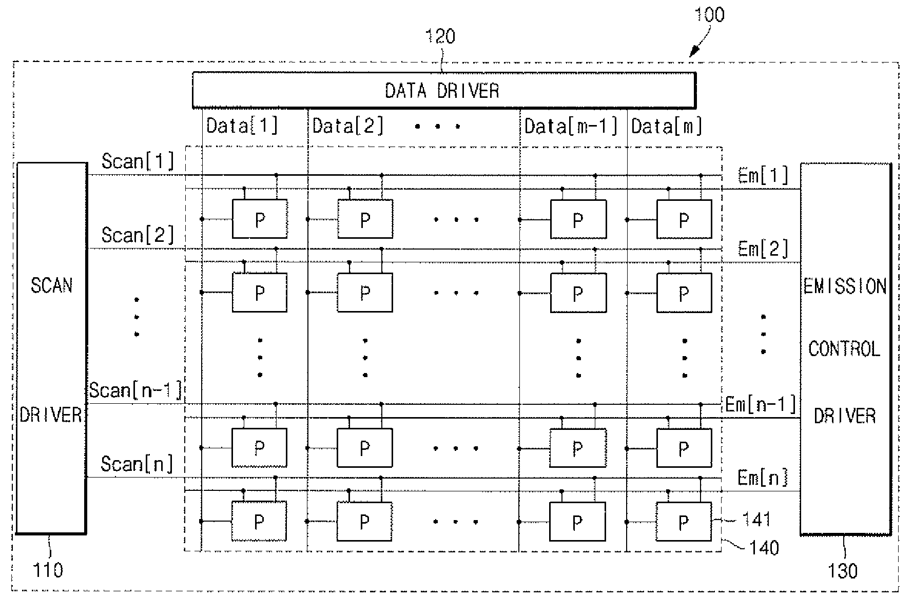
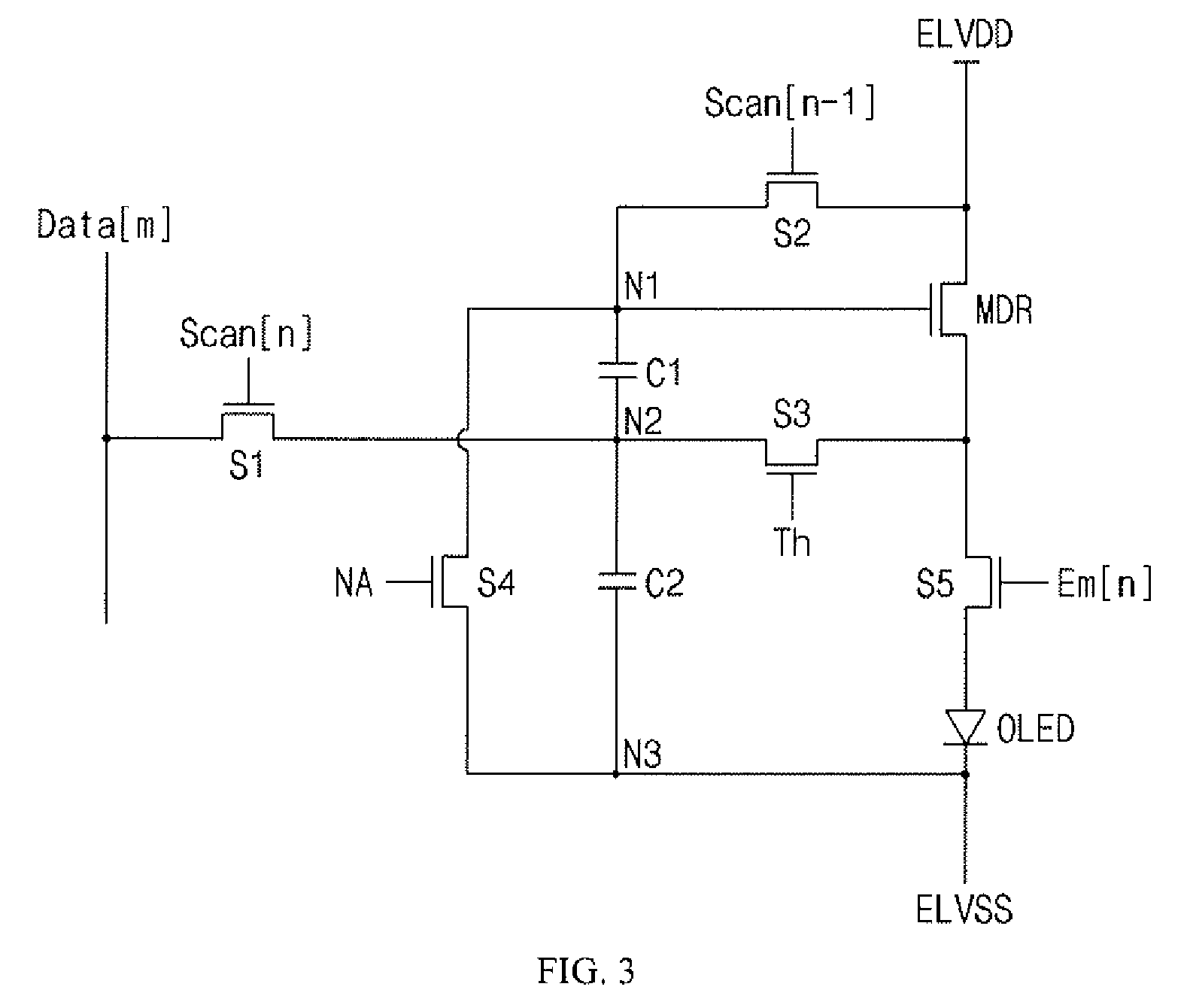
[0050]Hereinafter, preferred embodiments of the present invention will be described in detail with reference to the accompanying drawing. The aspects and features of the present invention and methods for achieving the aspects and features will be apparent by referring to the embodiments to be described in detail with reference to the accompanying drawings. However, the present invention is not limited to the embodiments disclosed hereinafter, but can be implemented in diverse forms. The matters defined in the description, such as the detailed construction and elements, are nothing but specific details provided to assist those of ordinary skill in the art in a comprehensive understanding of the invention, and the present invention is only defined within the scope of the appended claims. In the entire description of the present invention, the same drawing reference numerals are used for the same elements across various figures. In addition, a term of “electrically coupled” means not o...


PUM


Abstract

An organic light emitting display that can minimize degradation of a drive transistor comprising a first switching element whose control electrode is electrically coupled to a scan line, being electrically coupled between a data line and a first voltage line for transmitting a data signal; a drive transistor whose control electrode is electrically coupled to the first switching element, being electrically coupled between the first and second voltage lines; an organic light emitting diode electrically coupled to the drive transistor, displaying an image by a current supplied through the drive transistor; a first capacitive element electrically coupled between the control electrode of the drive transistor and the first switching element; a second capacitive element electrically coupled between the first capacitive element and the second voltage line; a second switching element electrically coupled between the first voltage line and the control electrode of the drive transistor; a third switching element electrically coupled between the first switching element and the drive transistor; a fourth switching element electrically coupled between the control electrode of the drive transistor and the second voltage line; and a fifth switching element electrically coupled between the drive transistor and the second voltage line.

Description

CROSS-REFERENCE TO RELATED APPLICATIONS[0001]This application is based on and claims priority to Korean Patent Application No. 10-2007-0073427 filed on Jul. 23, 2007 in the Korean Intellectual Property Office (KIPO), the entire contents of which are hereby incorporated by reference.BACKGROUND OF THE INVENTION[0002]1. Field of the Invention[0003]The present invention relates to an organic light emitting display, and more particularly, to an organic light emitting display that can minimize degradation of a drive transistor in a pixel circuit of the organic light emitting display and brightness change of an organic light emitting diode caused by the degradation.[0004]2. Description of the Related Art[0005]Generally, a conventional organic light emitting display is a display device emitting light by electrically exciting fluorescent or phosphorescent materials. The organic light emitting display displays images by driving N×M number of organic light emitting cells. The organic light emi...

Claims


Application Information

Patent Timeline
IPC IPC(8): G09G3/30
CPCG09G3/3233G09G2300/0819G09G2320/066G09G2300/0861G09G2320/0261G09G2300/0852G09G3/20G09G3/30G09G3/32H05B33/12
Inventor HAN, MIN KOOHAN, SANG MYEON
Owner SEOUL NAT UNIV R&DB FOUND
Why Eureka
Try Eureka