Threshold device for a memory array

a memory array and threshold device technology, applied in semiconductor devices, digital storage, instruments, etc., can solve problems such as unsatisfactory layout of three-terminal memory cells

Inactive Publication Date: 2009-01-29
UNITY SEMICON
View PDF39 Cites 129 Cited by
  • Summary
  • Abstract
  • Description
  • Claims
  • Application Information

AI Technical Summary

Problems solved by technology

However, the layout for three-terminal memory cells is not ideal and usually requires 8F2 for each memory cell in an array of memory cells, where F is the minimum feature size.

Method used


Image

  • Threshold device for a memory array
  • Threshold device for a memory array
  • Threshold device for a memory array

Examples


Embodiment Construction

[0057]In the following detailed description and in the several figures of the drawings, like elements are identified with like reference numerals.

Memory System Architecture

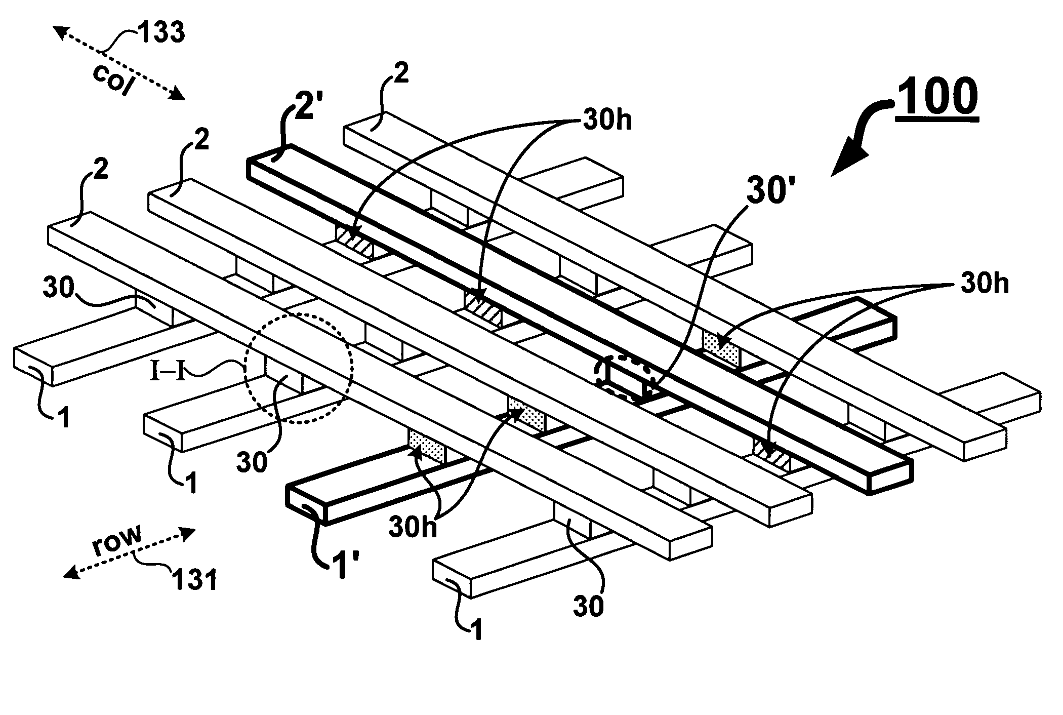
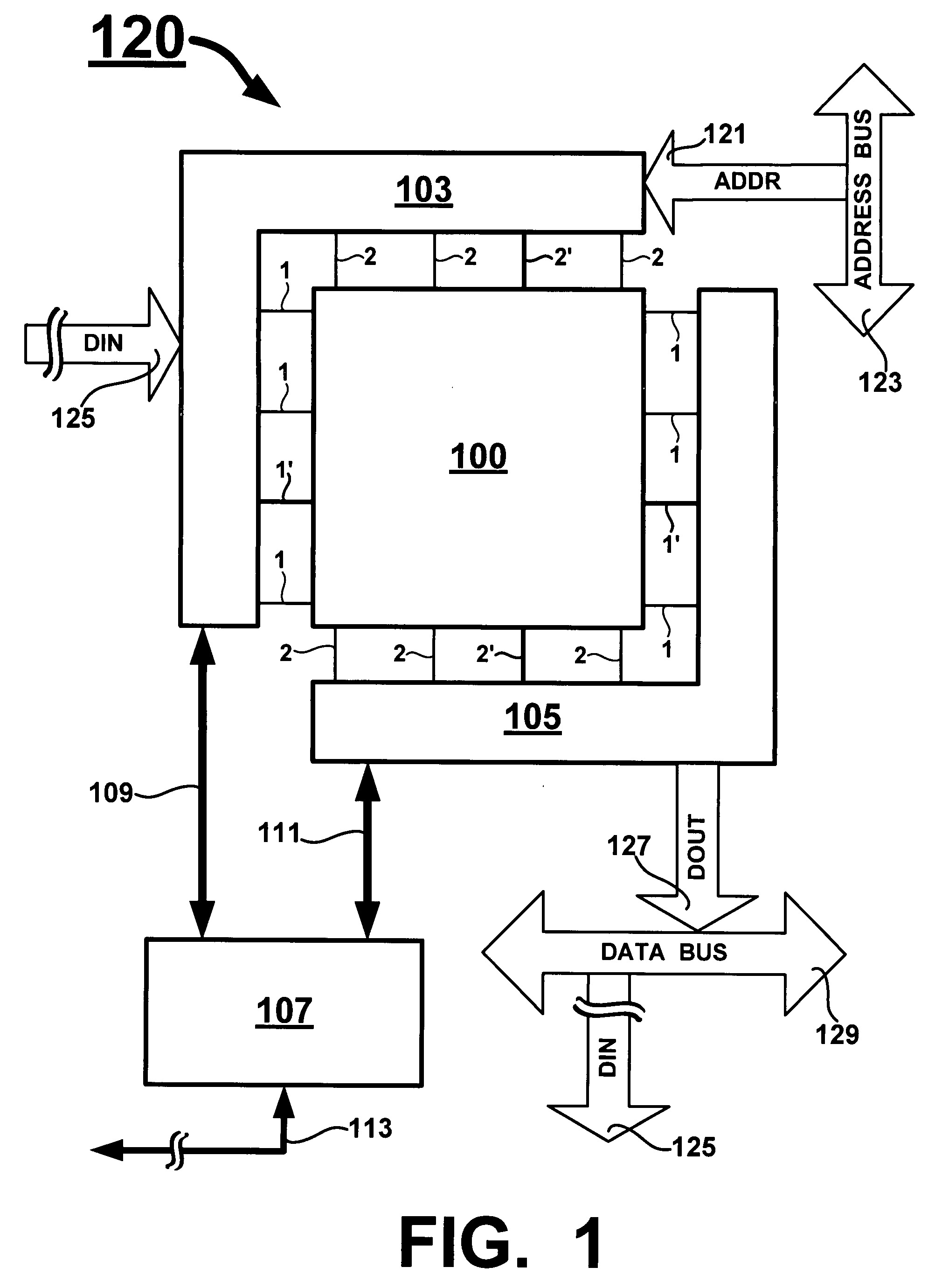
[0058]In FIG. 1, an exemplary memory system 120 includes a two-terminal cross-point memory array 100 (array 100 hereinafter) including a plurality of first conductive traces 1, a plurality of second conductive traces 2, an address unit 103, and a sense unit 105. The address unit 103 receives an address ADDR, decodes the address, and based on the address, selects at least one of the plurality of first conductive traces (denoted as 1′) and one of the plurality of second conductive traces (denoted as 2′). The address unit 103 applies select voltage potentials to the selected first and second conductive traces 1′ and 2′. The address unit 103 also applies a non-select voltage potential to unselected traces 1 and 2. The sense unit 105 senses one or more currents flowing through one or more of the conductive traces. Duri...


PUM


Abstract

A threshold device including a plurality of adjacent tunnel barrier layers that are in contact with one another and are made from a plurality of different dielectric materials is disclosed. A memory plug having first and second terminals includes, electrically in series with the first and second terminals, the threshold device and a memory element that stores data as a plurality of conductivity profiles. The threshold device is operative to impart a characteristic I-V curve that defines current flow through the memory element as a function of applied voltage across the terminals during data operations. The threshold device substantially reduces or eliminates current flow through half-selected or un-selected memory plugs and allows a sufficient magnitude of current to flow through memory plugs that are selected for read and write operations. The threshold device reduces or eliminates data disturb in half-selected memory plugs and increases S/N ratio during read operations.

Description

FIELD OF THE INVENTION[0001]This invention relates generally to semiconductors. More specifically, this invention relates to memory systems.BACKGROUND OF THE INVENTION[0002]A memory system may include sets of electrically conductive traces (e.g., word lines and bit lines) with a memory cell positioned at an intersection of a word line with a bit line. In some memory systems, a semiconductor device, such as a transistor, is positioned with and electrically coupled with the memory cell. The transistor includes a gate node (e.g., a MOSFET) or a base node (e.g., a bipolar transistor) coupled with a select line that controls access to the memory cell during data operations (e.g., read or write operations) to the memory cell. Furthermore, the transistor can be configured to require a range of threshold voltage potentials to be applied to the select line in order to read or write data to the memory cell. Accordingly, one range of threshold voltages can be used to read data from the memory ...

Claims


Application Information

Patent Timeline
Patent Type & Authority Applications(United States)
IPC IPC(8): G11C7/00
CPCG11C7/02G11C11/5685G11C13/0007G11C13/003G11C13/0069G11C2013/009H01L27/2481G11C2213/71G11C2213/76H01L45/08H01L45/1233H01L45/147H01L27/2418G11C2213/32H10B63/22H10B63/84H10N70/24H10N70/8836H10N70/826
Inventor BREWER, JULIE CASPERSONRINERSON, DARRELLCHEVALLIER, CHRISTOPHE J.KINNEY, WAYNELAMBERTSON, ROYSCHLOSS, LAWRENCE
Owner UNITY SEMICON
Why Eureka
Try Eureka