Apparatus and method of improving beam shaping and beam homogenization

a technology of apparatus and beam, which is applied in the direction of manufacturing tools, instruments, optical elements, etc., can solve the problems of only dissipating heat into the surrounding space or structures, limiting the speed of heat up and cooling down the wafer, and heating the entire wafer

a technology of apparatus and beam, which is applied in the direction of manufacturing tools, instruments, optical elements, etc., can solve the problems of only dissipating heat into the surrounding space or structures, limiting the speed of heat up and cooling down the wafer, and heating the entire wafer

US20090032511A1Active Publication Date: 2009-02-05APPLIED MATERIALS INC

Image

  • Apparatus and method of improving beam shaping and beam homogenization
  • Apparatus and method of improving beam shaping and beam homogenization
  • Apparatus and method of improving beam shaping and beam homogenization

Examples


Embodiment Construction

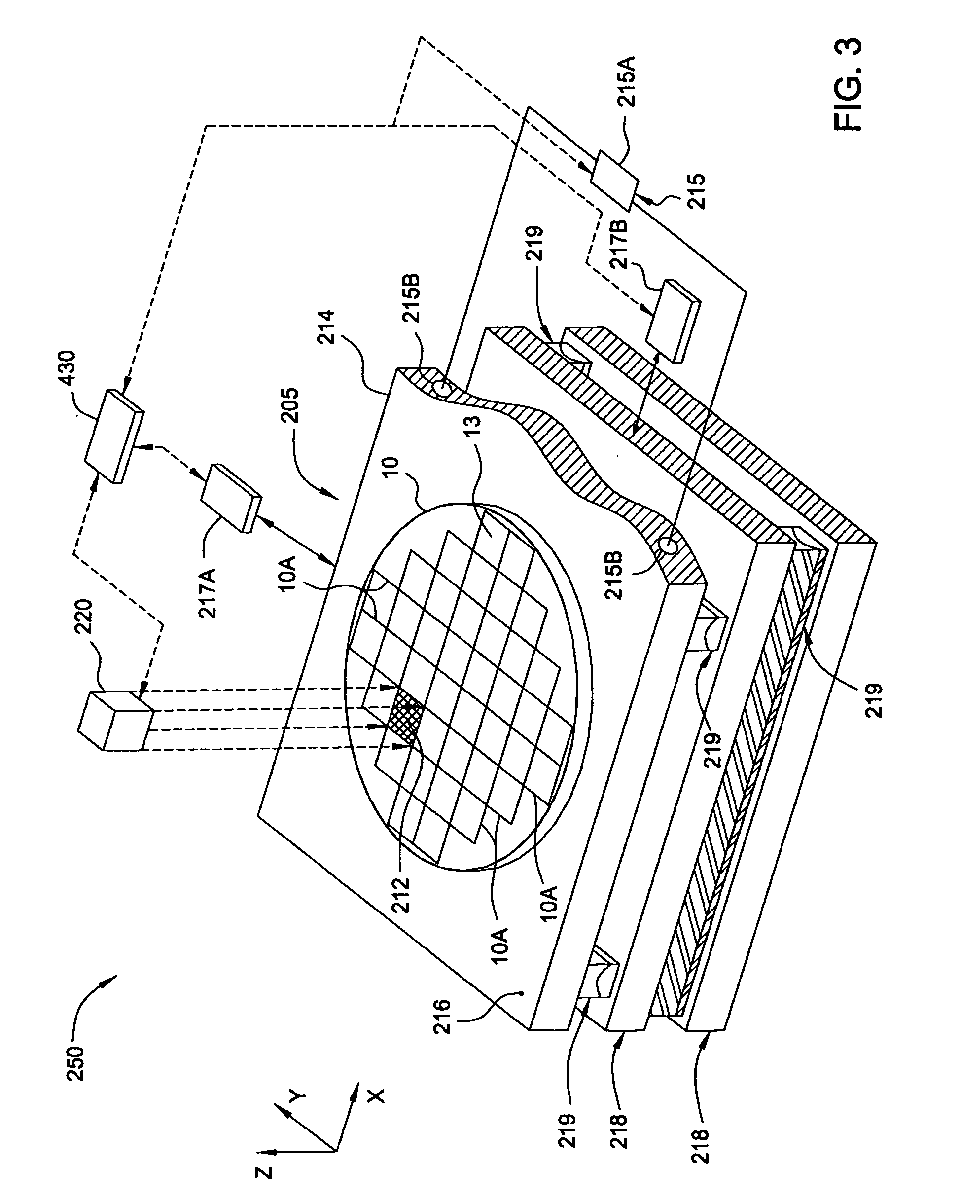
[0041]The present invention generally relates to an optical system that is able to reliably deliver a uniform amount of energy across an anneal region 212 (FIG. 3) contained on a surface of a substrate. In one embodiment, the optical system is adapted to deliver, or project a uniform amount of energy, or “image,” having a desired two-dimensional shape to a desired region on the surface of the substrate. Typically, the anneal regions 212 may be square or rectangular in shape and range in area between about 4 mm2 and about 1000 mm2. Generally, the optical system and methods of the present invention are used to preferentially anneal one or more regions found within the anneal regions 212 by delivering enough energy to cause the one or more regions to re-melt and solidify.

[0042]In general the term “substrates” as used herein can be formed from any material that can benefit from the pulse laser annealing process, such as a material that has some natural electrical conducting ability or a...


PUM

PropertyMeasurementUnit
wavelengthsaaaaaaaaaa
temperatureaaaaaaaaaa

Abstract

The present invention generally relates to an optical system that is able to reliably deliver a uniform amount of energy across an anneal region contained on a surface of a substrate. The optical system is adapted to deliver, or project, a uniform amount of energy having a desired two-dimensional shape on a desired region on the surface of the substrate. Typically, the anneal regions may be square or rectangular in shape. Generally, the optical system and methods of the present invention are used to preferentially anneal one or more regions found within the anneal regions by delivering enough energy to cause the one or more regions to re-melt and solidify.

Description

CROSS-REFERENCE TO RELATED APPLICATIONS[0001]This application is related to the U.S. Patent Application entitled “Method For Partitioning And Incoherently Summing A Coherent Beam” by Dean Jennings et al. [Docket #APPM 11313], filed Jul. 31, 2007, and the U.S. Patent Application entitled “Method And Apparatus For Decorrelation Of Spatially And Temporally Coherent Light” by Dean Jennings et al. [Docket #APPM 11369], filed Jul. 31, 2007, which are all herein incorporated by reference.BACKGROUND OF THE INVENTION[0002]1. Field of the Invention[0003]Embodiments of the present invention generally relate to an apparatus and method used to manufacture a semiconductor device. More particularly, the invention is directed to an apparatus and method that is used to thermally process a substrate.[0004]2. Description of the Related Art[0005]The integrated circuit (IC) market is continually demanding greater memory capacity, faster switching speeds, and smaller feature sizes. One of the major steps...

Claims


Application Information

Patent Timeline
05 Feb 2009
Publication
US20090032511A1
IPC
B23K26/06; G02B27/10
CPC
B23K26/0604; B23K26/0613; B23K26/063; B23K26/073; B23K26/0732; G02B27/0961; B23K26/067; B23K26/0622
Inventors
ADAMS, BRUCE E.; HOWELLS, SAMUEL C.