

Magnetic field detecting element having thin stack with a plurality of free layers and thick bias magnetic layer
a magnetic layer and detector element technology, applied in the field of magnetic field detecting elements, can solve the problems of large limitation that originates from the layer configuration of the conventional cpp elements, restricts the reduction of the thickness of the spin-valve film, and limits the magnetization of the pinned layer as a whole, so as to achieve sufficient bias magnetic field and reduce the gap between the shields
- Summary
- Abstract
- Description
- Claims
- Application Information
AI Technical Summary
Benefits of technology
Problems solved by technology
Method used
Image

Examples
Embodiment Construction
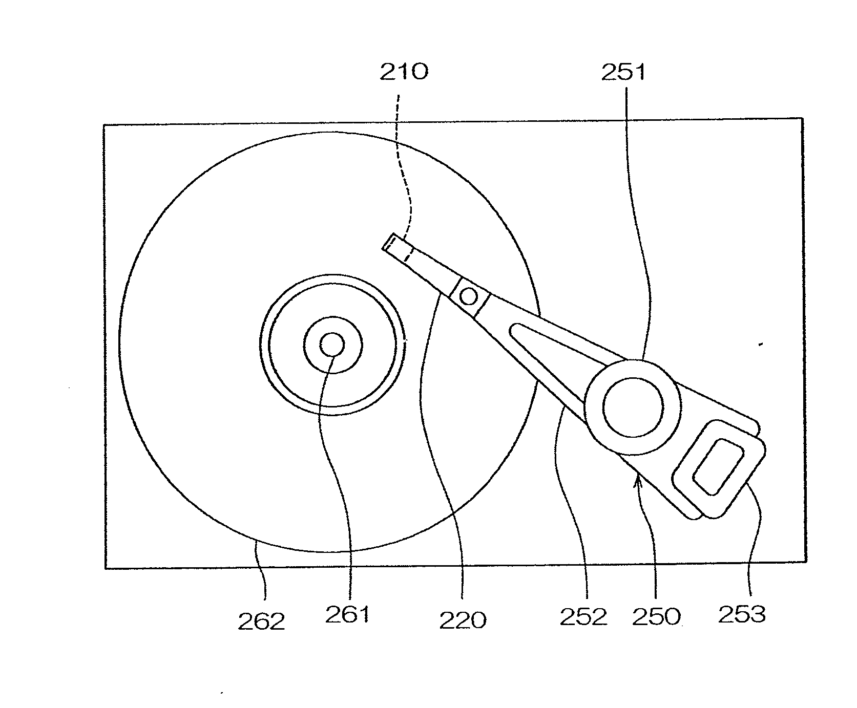
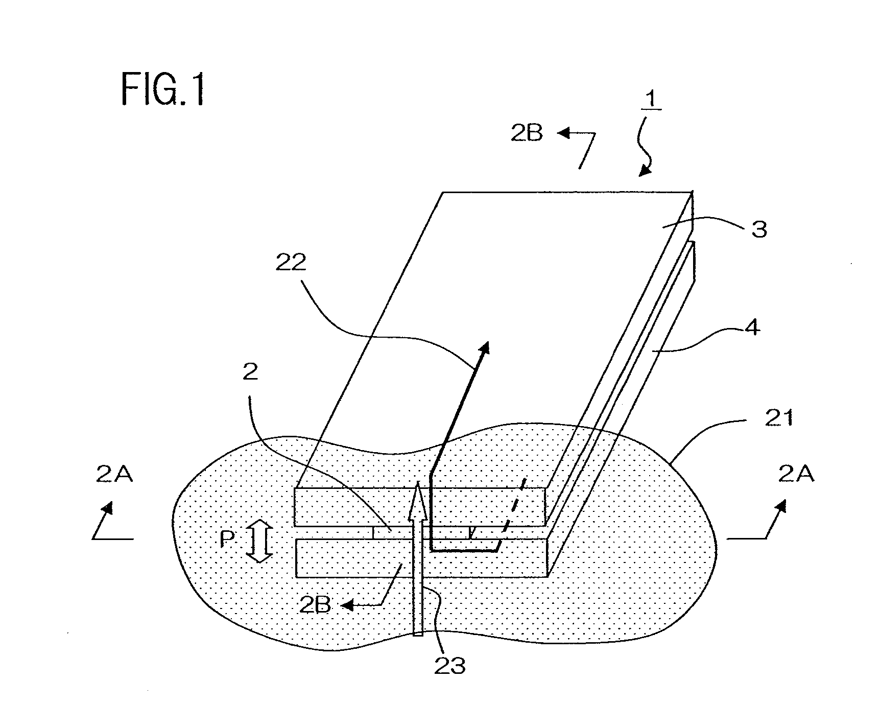
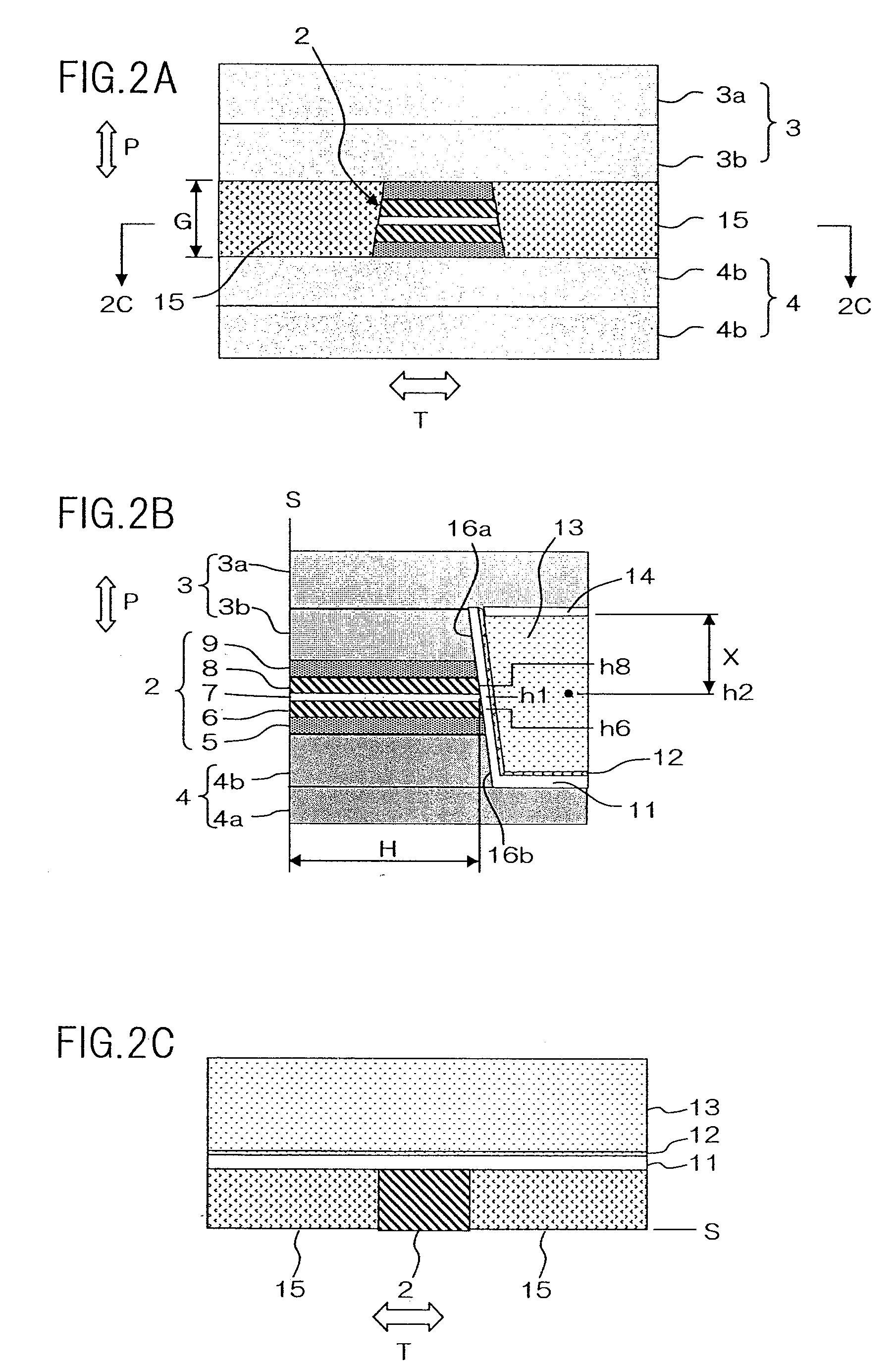
[0030]An embodiment of the present invention will now be described with reference to the attached drawings. A magnetic field detecting element of the present embodiment is particularly suitable for use as a read head portion of a thin film magnetic head of a hard disc drive. FIG. 1 is a conceptual perspective view of a magnetic field detecting element of the present embodiment. FIG. 2A is a side view of the magnetic field detecting element when viewed from 2A-2A direction of FIG. 1, i.e., viewed from the air bearing surface. FIG. 2B is a cross sectional view of the magnetic field detecting element taken along 2B-2B line of FIG. 1. FIG. 2C is a cross sectional view of the magnetic field detecting element taken along 2C-2C line of FIG. 2A. The air bearing surface refers to the surface of magnetic field detecting element 1 that faces recording medium 21.
[0031]Magnetic field detecting element 1 includes stack 2, upper shield electrode layer 3 and lower shield electrode layer 4 which are...
PUM
| Property | Measurement | Unit |
|---|---|---|
| thickness | aaaaa | aaaaa |
| thickness | aaaaa | aaaaa |
| thickness | aaaaa | aaaaa |
Abstract
Description
Claims
Application Information