

Method and Apparatus for Patterning a Conductive Layer, and a Device Produced Thereby
a technology of conductive layer and patterning method, which is applied in the manufacture of electrode systems, electric discharge tubes/lamps, discharge tubes luminescnet screens, etc., can solve the problems of lack of patterning methods, slow and costly, and technique is not well suited for roll-to-roll production
Inactive Publication Date: 2009-02-12
CIBA SPECIALTY CHEM CORP
View PDF9 Cites 39 Cited by
- Summary
- Abstract
- Description
- Claims
- Application Information
AI Technical Summary
Benefits of technology
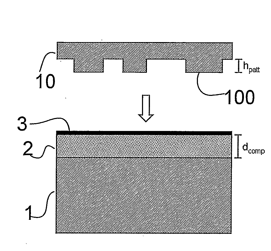
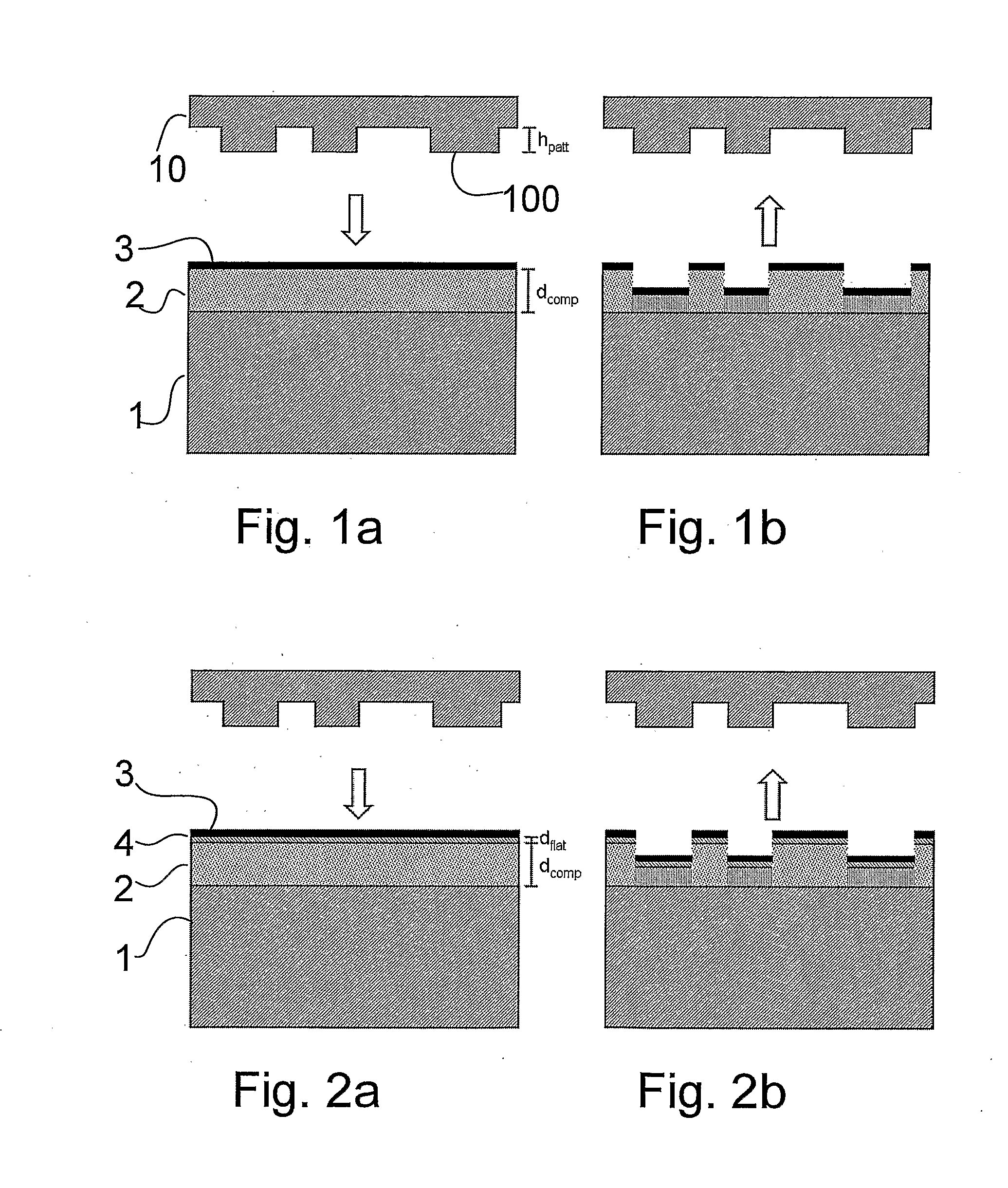
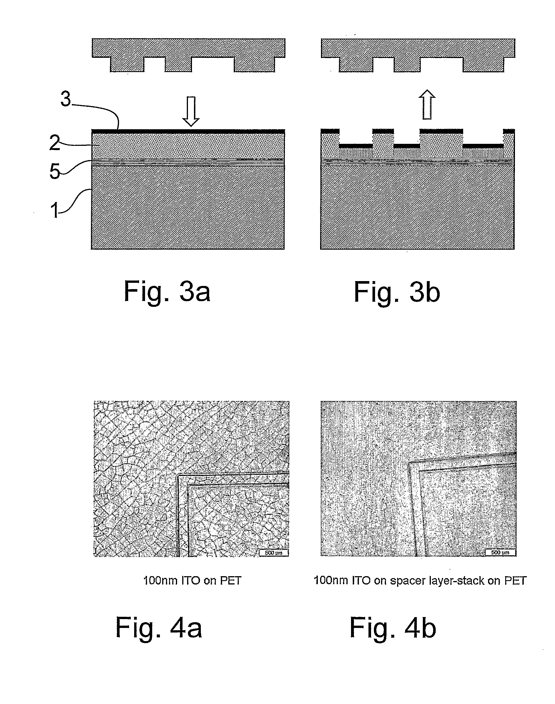
The present invention provides a method of patterning conductive layers or layers stacks in organic devices by embossing a compressible layer between the substrate and the conductive layer. This method eliminates the drawbacks of previous methods and provides better results. The invention also provides organic devices with patterned conductive layers made using this method. The compressible layer can be a low density polymer or a mixture of low density polymer and inorganic material. The invention can be used in various organic devices such as OLEDs, OFETs, or organic photocells.
Problems solved by technology
Up to now there is a lack of patterning methods which address all the points mentioned above.
On the other hand the multiple steps of the process make it very slow and costly.
Thus this technique is not well suitable for roll-to-roll production.
The drawback of the printing approach is the limitation of the resolution of the printing processes.
Especially patterned layers of about 100 nm with a well defined thickness at the edges of the pattern are difficult to realise.
Due to the heat that is introduced in the layer or layer stack and / or the substrate the method alters or damages the layers or the substrate.
Furthermore the technique is up to now not fast enough to be implemented in a roll-to-roll process and the investment and thus the costs are rather high.
The drawback of this technique is the limited resolution of larger than 200 μm.
The method is well suited for the mentioned applications but is inapplicable for patterning of conductive layers used in organic devices due to the deformation of the substrate.
The described method does not solve the problem of damaging the substrate by cutting through the layer or layers.
Further no solution is provided for the problem of damaging the substrate and / or the deposited conductive layer due to the material flow during the embossing step.
A drawback of this patent application is that before the die can be reused it must be cleaned in an additional step.
This slows down the speed of the process and increases the costs.
This release function lowers the stability of the layer setup distinctly and limits the possible material combinations.
Method used
View moreImage
Smart ImageViewing Examples

Examples
examples
[0046]The following examples illustrate the invention. The invention is not limited to these examples.
Login to View More PUM
| Property | Measurement | Unit |
|---|---|---|
| thickness | aaaaa | aaaaa |
| thickness | aaaaa | aaaaa |
| thickness | aaaaa | aaaaa |
Abstract
A device is fabricated by a method in which a conductive layer or layer stack is formed over a compressible layer or layer stack, and contacted with an embossing tool. Raised portions of the embossing tool compress the compressible layer or stack and countersink the conductive layer or stack into the compressible layer or stack.
Description
FIELD OF THE INVENTION[0001]The invention relates to the production of organic devices in general and is more particularly related to the patterning of conductive layers used in such organic devices like e.g. organic light emitting devices (OLEDs), organic field effect transistors (OFETs) or organic photocells.[0002]1. Background of the Invention[0003]The rapid development of organic device technology increases the need for fast and cheap but reliable methods for the deposition of the desired layers as well as for the patterning of the layers, especially of the conductive layers. Methods for production of large areas are needed. Roll-to-roll processes with polymeric substrates are a promising approach. Due to the low stability of the organic semi-conducting and conducting materials against oxygen and water for most applications good barrier properties of the substrate are needed. Therefore often barrier coatings are deposited on polymeric substrates prior to the deposition of the la...
Claims
Login to View More Application Information
Patent Timeline
 Patent Type & AuthorityApplications(United States)
IPC IPC(8): H01L51/00H01L51/40H01J9/24B44B5/00H01J1/63H01L51/05H10K99/00
CPCH01L51/0015H01L51/0023H01L51/0036Y02E10/549H01L51/0512H01L51/56H01L2251/105H01L51/0086H10K71/211H10K71/621H10K85/113H10K85/344H10K10/462H10K71/821H10K71/40H10K2102/351H10K71/00
InventorWALTER, HARALDBEIERLEIN, TILMAN
OwnerCIBA SPECIALTY CHEM CORP