Light source, manufacturing method of light source, lighting apparatus, and display apparatus

a manufacturing method and technology for light sources, applied in the direction of semiconductor devices for light sources, lighting and heating devices, planar light sources, etc., can solve the problems of conductivity failure, bump in very weak bonding, led bare chips may stop lighting up, etc., to enhance the conductivity and enhance the bonding reliability of the smaller-area electrod

Active Publication Date: 2009-02-12
PANASONIC CORP
View PDF3 Cites 52 Cited by
  • Summary
  • Abstract
  • Description
  • Claims
  • Application Information

AI Technical Summary

Benefits of technology

[0036]In the light source according to the present invention, the bump that bonds the smaller-area electrode and a corresponding conductive land will not be the smallest of all the bumps. Therefore, compared to a conventional light source where the bump that bonds the smaller-area electrode and a corresponding conductive land may be the smallest of all the bumps, bonding force between the smaller-area electrode and a corresponding conductive land is enhanced, thereby reducing the possibility of causing non-lighting of the light emitting device.
[0037]In particular, in a case where the smaller-area electrode and a conductive land is bonded by only one bump, the bump that is bonded with an electrode and with a conductive land in the smallest area of all the plurality of bumps will never be used to bond the smaller-area electrode. In other words, a bonded area of a bump used for the smaller-area electrode is always larger than a bonded area of the bump having the smallest bonded area among the larger-area electrode. Accordingly, even if the number of bumps used to bond the smaller-area electrode is small, it is possible to enhance the bonding reliability of the smaller-area electrode. In addition, the conductivity reliability of the smaller-area electrode is enhanced as well.
[0038]In a case where a bump having the largest bonded area both with an electrode and with a conductive land is used to bond the smaller-area electrode, it is natural that the bonded area of the bump is the largest among all the bumps. Accordingly, even when only the bump is used to bond the smaller-area electrode, it is possible to enhance the conductivity reliability of the smaller-area electrode.
[0039]In addition, a bonded area of a bump having the largest bonded area with an electrode and with a conductive land is 1.2 times a bonded area of any of the rest of the bumps, or even more. This leads to enhanced bonding reliability.
[0040]On the other hand, according to a manufacturing method of a light source according to the present invention, the size of the bumps differs between the electrodes. Therefore, it is possible to enhance the bonding force between the electrode and the conductive land for the smaller-area electrode, for example by bonding the smaller-area electrode using a bump larger than bumps used to bond the larger-area electrode. This helps reduce the possibility of non-lighting of the light emitting device.

Problems solved by technology

However, even for a light source for LED that has passed the test, with years of use, its LED bare chips may stop lighting up, due to conductivity failure between the LED bare chips and the bumps, or between the bumps and the conductive lands.
In such a case, the bump in very weak bonding has a possibility of coming off with years of use.
However, if this bump is on the n-electrode, it is quite likely to cause conductivity failure between the LED bare chip and the conductive lands, leading to non-lighting of the LED bare chip.
Note that, although with a lower possibility, this problem pertaining to the conductivity failure also arises in a case where more than one bump is used with respect to an n-electrode.

Method used


Image

  • Light source, manufacturing method of light source, lighting apparatus, and display apparatus
  • Light source, manufacturing method of light source, lighting apparatus, and display apparatus
  • Light source, manufacturing method of light source, lighting apparatus, and display apparatus

Examples


first embodiment

[0173]In particular, the present LED bare chip is larger than the LED bare chip in the first embodiment, with one side of the bottom surface having a length of 1 mm (in comparison, one side of the bottom surface of the LED bare chip has a length of 0.3 μm). Accordingly, the distance between adjacent bumps 191a tends to be large. When the distance between adjacent bumps 191a becomes large in this way, uniform electric current density tends to be impaired, due to positions of the bumps 191a in the p-electrode 2Lpa. Accordingly, the brightness variations tend be more obvious. Therefore, for an LED bare chip having a large light emitting area, it is considered effective to arrange bumps at the side of the p-electrode in an orderly formation, for the purpose of maintaining uniform heat dissipation characteristics of the surface, as counter measures against the brightness variation problem.

example 2

[0174](B) Example 2

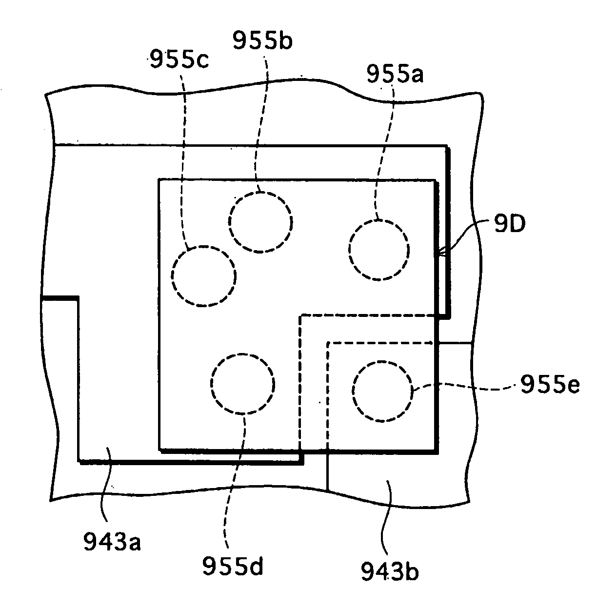
[0175]FIG. 15B shows an LED bare chip 2Db according to the example 2 in the modification example 3. As FIG. 15B shows, the structures of the LED bare chip 2Db are substantially the same as in the example 1, such as in form and size of the bottom surface, and a ratio between the area of the n-electrode and the area of the p-electrode. However, in the example 2, two bumps 192b exist for the n-electrode 2Lnb, and 26 bumps 191b exist for the p-electrode 2Lpb. The bumps 191b are arranged in an orderly formation. The cross sections of the bumps 191b and of the bumps 191a are substantially round, respectively. With regard to a cross sectional area for each bump, the cross sectional area 2Snb of one bump 192b is larger than the cross sectional area 2Spb of one bump 191b.

example 3

[0176](C) Example 3

[0177]FIG. 15C shows an LED bare chip 2Dc according to the example 3 of the modification example 3. As FIG. 15C shows, the structures of the LED bare chip 2Dc are substantially the same as in the example 1, such as in form and size of the bottom surface, and a ratio between the area of the n-electrode and the area of the p-electrode. However, the example 3 is different from the examples 1 and 2, in that an n-electrode 2Lnc exists like an island in the substantial center of the bottom surface of the LED bare chip 2Dc. In the example 3, one bump 192c exists for the n-electrode 2Lnc, and 32 bumps 191c exists for the p-electrode 2Lpc. The bumps 191c are arranged in an orderly formation. With regard to the cross sectional area of each bump, the cross sectional area 2Snc of the bump 192c is larger than the cross sectional area 2Spc of one bump 191c. [0178]5. Substrate

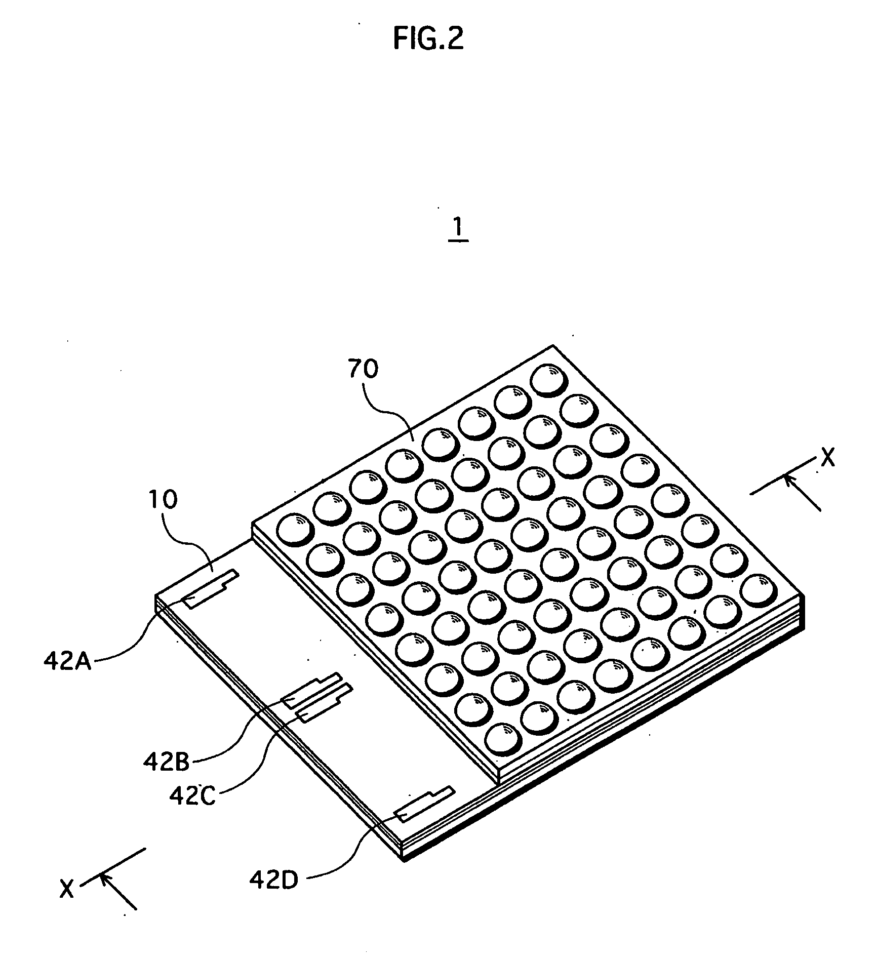
[0179]In the embodiment, the substrate 10 is for mounting thereon a plurality of LED bare chips Dnm, how...


PUM


Abstract

Provided is a light source that has high reliability and hardly causes conductivity failure between a light emitting device and a conductive land. In an LED light source of the present invention, an LED bare chip is mounted to conductive lands of a substrate, using bumps (55a, 55b). The LED bare chip (D65) is provided with a p-electrode (Lp) and an n-electrode (Ln) on a rear surface. The p-electrode (Lp) is larger in area than the n-electrode (Ln). The p-electrode (Lp) is bonded to a corresponding conductive land via four bumps (55a), whereas the n-electrode (Ln) is bonded to a corresponding conductive land via one bump (55b). A bonded area (Sn) between the n-electrode (Ln) and the bump (55b) is larger than a bonded area (Sp) between the p-electrode (Lp) and one of the bumps (55a).

Description

TECHNICAL FIELD[0001]The present invention relates to a light source in which a light-emitting device, which has two electrodes on the rear surface, is mounted to a conductive land of a substrate via a plurality of bumps, and to a manufacturing method of the light source. The present invention also relates to a lighting apparatus and a display apparatus that employ the light source.BACKGROUND ART[0002]In recent years, light-emitting diode bare chips (hereinafter “LED bare chip”) are attracting attention, further high efficiency and long life compared to incandescent lamps and halogen lamps. Furthermore, with their small size, the LED bare chips are expected to realize small light sources.[0003]One example of light source realized using such LED bare chips is disclosed in Japanese laid-open patent application H08-37357. In the disclosed light source, an LED bare chip, which has two electrodes on the rear surface, is mounted to a conductive land of a substrate via a plurality of bumps...

Claims


Application Information

Patent Timeline
Patent Type & Authority Applications(United States)
IPC IPC(8): H01L33/00F21V19/00F21Y101/02H01L33/48
CPCF21K9/00F21Y2105/001H01L33/38H01L33/62H01L2224/1134H01L2924/01002H01L2924/01013H01L2924/01015H01L2924/01074H01L2924/01078H01L2924/01079H01L2924/01082H01L2924/09701H01L2924/00013H01L2924/01005H01L2924/01006H01L2924/01023H01L2924/01033H01L24/11F21Y2101/02H01L2924/12041H01L2224/13099F21K9/90F21V5/007F21K9/20F21K9/233F21Y2105/10F21Y2115/10F21V5/10H01L2924/00011H01L2924/00014H01L2924/12042H01L2924/15787H01L2924/00H01L2224/0401
Inventor UEMOTO, TAKAARINAITO, HIROYUKI
Owner PANASONIC CORP
Why Eureka
Try Eureka