

Semiconductor memory device
a memory device and semiconductor technology, applied in the field of semiconductor memory devices, can solve the problems of not being able to achieve a sufficiently large reference potential, requiring a longer test time, and not being able to meet the requirements of mass-storage ferroelectric memories
- Summary
- Abstract
- Description
- Claims
- Application Information
AI Technical Summary
Benefits of technology
Problems solved by technology
Method used
Image

Examples
first embodiment
(Configuration of Semiconductor Memory Device of First Embodiment)
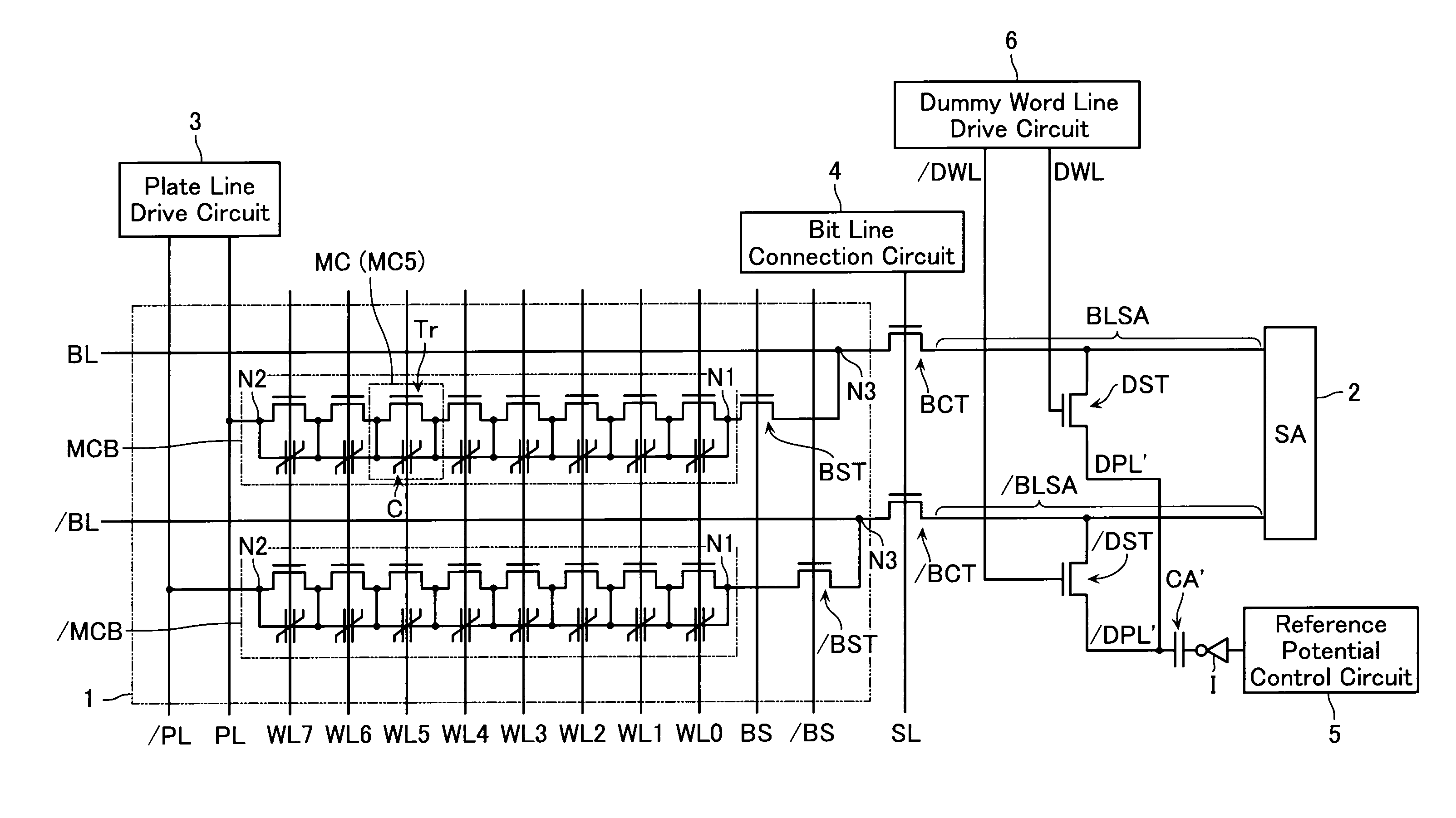
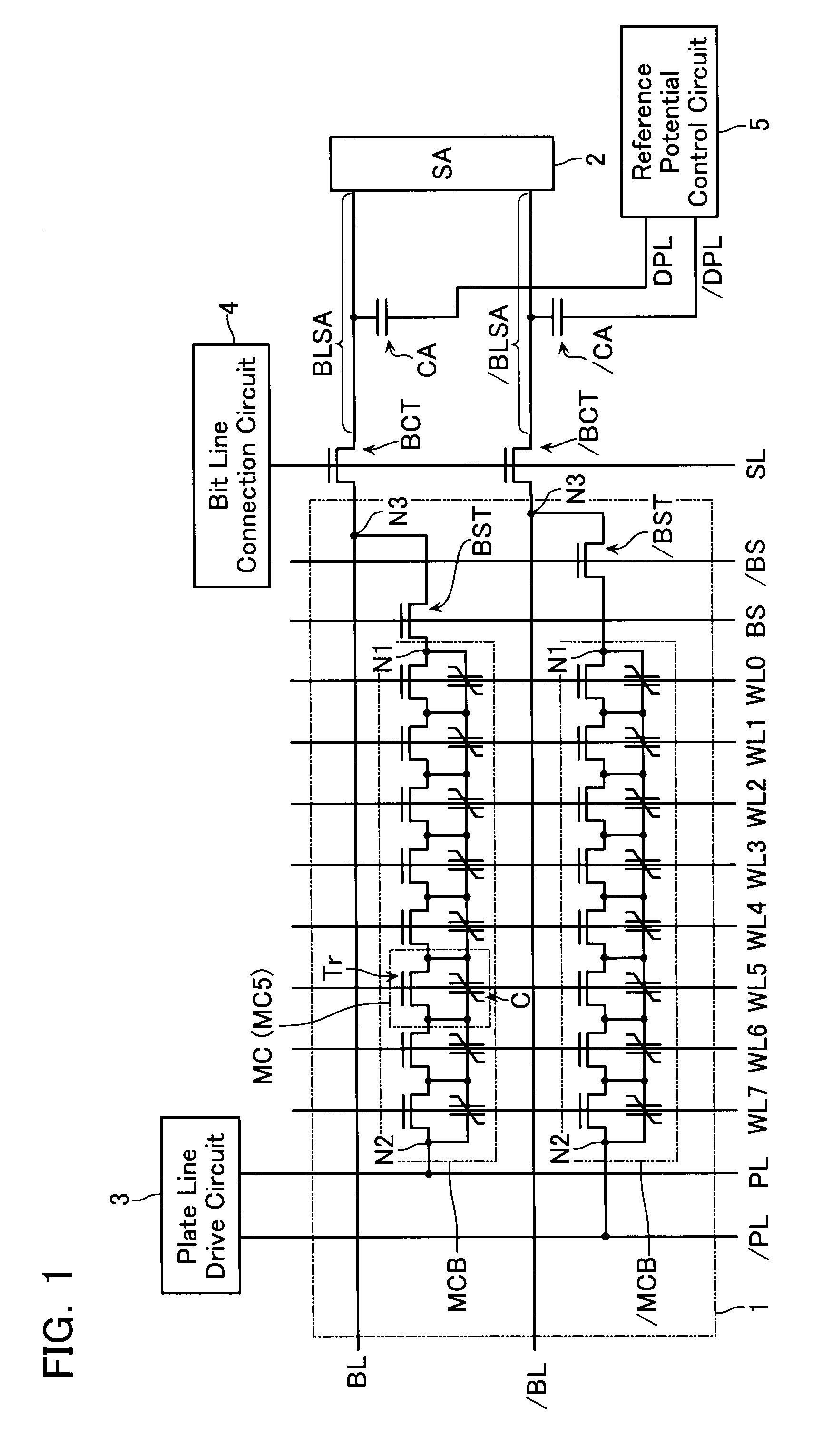
[0019]FIG. 1 is a block diagram of a semiconductor memory device (FeRAM) according to a first embodiment of the present invention. The semiconductor memory device according to the first embodiment comprises a memory cell array 1, a sense amp circuit 2, a plate line drive circuit 3, a bit line connection circuit 4, and a reference potential control circuit 5. The sense amp circuit 2, the plate line drive circuit 3, the bit line connection circuit 4 and the reference potential control circuit 5 have functions of controlling the potentials on signal lines connected to the memory cell array 1 at “High” and “Low”.
[0020]The memory cell array 1 comprises a memory cell MC including a ferroelectric capacitor C and a transistor Tr. In the memory cell MC the ferroelectric capacitor C and the transistor Tr are connected in parallel. In the shown example, such eight memory cells MC are connected in series to configure a cell block...
second embodiment
(Configuration of Semiconductor Memory Device of Second Embodiment)
[0031]Referring next to FIG. 3, a semiconductor memory device according to a second embodiment of the present invention is described. FIG. 3 is a block diagram of the semiconductor memory device (FeRAM) according to the second embodiment of the present invention. In the second embodiment the same elements as those in the first embodiment are denoted with the same reference numerals and omitted from the following description.
[0032]The above-described semiconductor memory device according to the first embodiment reduces the area occupied by the dummy capacitors CA, / CA. On the other hand, the capacities of the bit lines BL, / BL are small (because they are only the partial bit lines BLSA, / BLSA) and accordingly α rays may cause failed program possibly. The semiconductor memory device according to the second embodiment eliminates such the problem about the first embodiment.
[0033]The semiconductor memory device according ...
third embodiment
(Configuration of Semiconductor Memory Device of Third Embodiment)
[0047]Referring next to FIG. 7, a semiconductor memory device according to a third embodiment of the present invention is described. FIG. 7 is a block diagram of the semiconductor memory device (FeRAM) according to the third embodiment of the present invention. In the third embodiment the same elements as those in the second embodiment are denoted with the same reference numerals and omitted from the following description.
[0048]In the semiconductor memory device according to the third embodiment, the reference potential control circuit 5 is connected to one end of the dummy capacitor CA′ via an inverter I. The inverter I is provided in connection with one end of the dummy capacitor CA′ on the side not connected to the bit lines BL, / BL.
[0049]The other end of the dummy capacitor CA′ is connected to the dummy plate lines PL, / PL. The dummy plate lines PL, / PL are connected to the bit lines BL, / BL via the dummy capacito...
PUM
 Abstract
Description
Claims
Application Information