Non-volatile memory device and method of fabricating the same

Inactive Publication Date: 2009-02-19
SAMSUNG ELECTRONICS CO LTD
View PDF10 Cites 13 Cited by
  • Summary
  • Abstract
  • Description
  • Claims
  • Application Information

AI Technical Summary

Benefits of technology

[0019]Accordingly, the non-volatile memory device according to example embodiments may increase integration density and/or prevent short channel effect by reducing the width of and the distance between the fins, thereby reducing leakage current and off-current.
[0020]Furthermore, the non-volatile memory device may easily control a coupling ratio, which may be defined as a ratio between a voltage applied to the control gate electrode to a

Problems solved by technology

However, because the conventional planar non-volatile memory devices are limited as to how much their integration may increase, the planar conventional non-volatile memory devices are limited in capacity and/or speed.
However, when the coupling ratio is increased by increasing the height of the floating gate electrode, the area of the floating gate electrode between adjacent cells may be in

Method used


Image

  • Non-volatile memory device and method of fabricating the same
  • Non-volatile memory device and method of fabricating the same
  • Non-volatile memory device and method of fabricating the same

Examples


Embodiment Construction

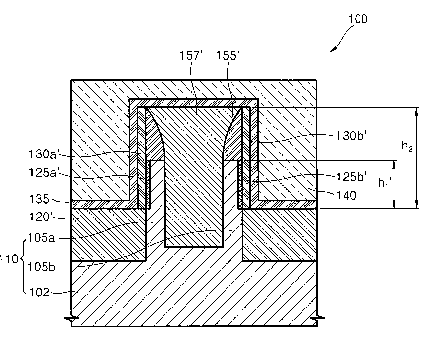
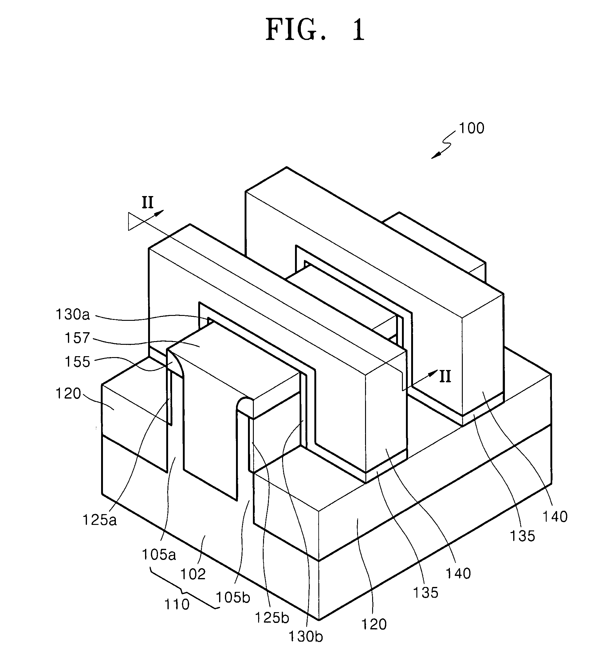
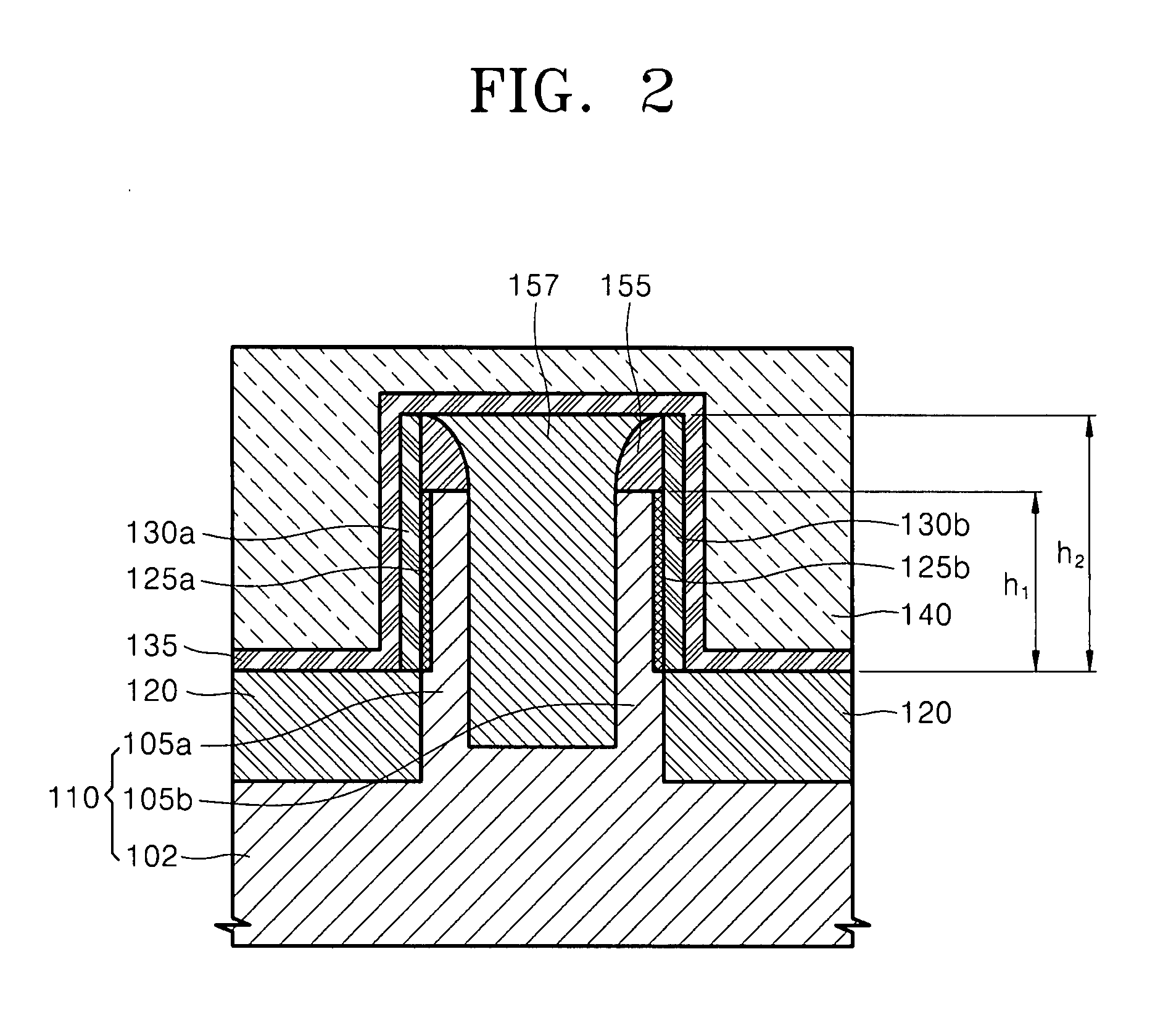
[0028]Example embodiments will now be described more fully with reference to the accompanying drawings, in which example embodiments are shown. The invention may, however, be embodied in many different forms and should not be construed as being limited to the embodiments set forth herein; rather these embodiments are provided so that this disclosure will be thorough and complete, and will fully convey the concept of the invention to those skilled in the art. In the drawings, the thicknesses of layers and regions are exaggerated for clarity.

[0029]Example embodiments will now be described more fully hereinafter with reference to the accompanying drawings. Embodiments may, however, be in many different forms and should not be construed as being limited to the example embodiments set forth herein. Rather, these example embodiments are provided so that this disclosure will be thorough and complete, and will fully convey the scope to those skilled in the art. In the drawings, the thicknes...


PUM


Abstract

Provided are a non-volatile memory device, which may have higher integration density, improved or optimal structure, and/or reduce or minimize interference between adjacent cells without using an SOI substrate, and a method of fabricating the non-volatile memory device. The non-volatile memory device may include: a semiconductor substrate comprising a body, and a pair of fins protruding from the body; a buried insulating layer filling between the pair of fins; a pair of floating gate electrodes on outer surfaces of the pair of fins to a height greater than that of the pair of fins; and a control gate electrode on the pair of floating gate electrodes.

Description

PRIORITY STATEMENT[0001]This application claims the benefit of Korean Patent Application No. 10-2007-0081460, filed on Aug. 13, 2007, in the Korean Intellectual Property Office, the disclosure of which is incorporated herein in its entirety by reference.BACKGROUND[0002]1. Field[0003]Example embodiments relate to a semiconductor device, for example, to a fin-type non-volatile memory device.[0004]2. Description of the Related Art[0005]As dimensions and operation speeds of semiconductor products decrease and increase, respectively, the operation speed and integration of non-volatile memory devices used for semiconductor products have increased. For example, flash memory devices have been used as higher-speed and higher-integrated non-volatile memory devices.[0006]Conventional planar non-volatile memory devices are structured such that a floating gate electrode and a control gate electrode are stacked. However, because the conventional planar non-volatile memory devices are limited as t...

Claims


Application Information

Patent Timeline
IPC IPC(8): H01L29/788H01L21/336
CPCH01L27/115H01L27/11521H01L29/7881H01L29/66825H01L29/785H01L29/66795H10B69/00H10B41/30H10B41/35H01L21/28141
Inventor KOO, JUNE-MOKIM, SUK-PILJIN, YOUNG-GUKIM, WON-JOOYOO, IN-KYEONGPARK, YOON-DONG
Owner SAMSUNG ELECTRONICS CO LTD
Why Eureka
Try Eureka