LED device having improved contrast

a technology of led devices and contrast, which is applied in the manufacture of electrode systems, electric discharge tubes/lamps, discharge tubes luminescnet screens, etc., can solve the problems of poor ambient contrast ratio, insufficient contrast of polarizers, and difficulty in achieving ambient contrast. , to achieve the effect of increasing the light output and ambient contrast of an led devi

Active Publication Date: 2009-02-26
GLOBAL OLED TECH
View PDF16 Cites 138 Cited by
  • Summary
  • Abstract
  • Description
  • Claims
  • Application Information

AI Technical Summary

Problems solved by technology

Similarly, inorganic LED devices, for example comprising quantum dots in a polycrystalline semiconductor matrix, located between a reflective electrode and a transparent or semi-transparent electrode, suffer from ambient contrast concerns.
Because LED devices typically employ a reflective back electrode, providing a good ambient contrast ratio can be problematic.
However, while effective in reducing reflections in high-ambient light conditions, for example, outdoors on sunny days, such polarizers do not always provide adequate contrast and they absorb more than half of the emitted light.
While such designs are useful, they require a patterned organic material deposition technology that is difficult to scale to large substrates.
Moreover, microcavity devices typically suffer from an unacceptable angular dependence on color.
However, while useful, such an approach does not improve the manufacturability of the device and provides inadequate contrast ratio under some illumination conditions.
Such designs, however, may have increased manufacturing costs, lower light output than desired, and reflectance larger than may be desired, as well as significant color change with changes in viewing angle.
Again such designs may have increased manufacturing costs and reflectance larger than may be desired.
However, this design employs a patterned semi-transparent electrode that can be difficult to manufacture in a top-emitting format.
Moreover, applicants have determined that color purity may be reduced in such a design and reflectance will likely be larger than desired.
However, the use of color filters substantially reduces the efficiency of the device.

Method used


Image

  • LED device having improved contrast
  • LED device having improved contrast
  • LED device having improved contrast

Examples


Embodiment Construction

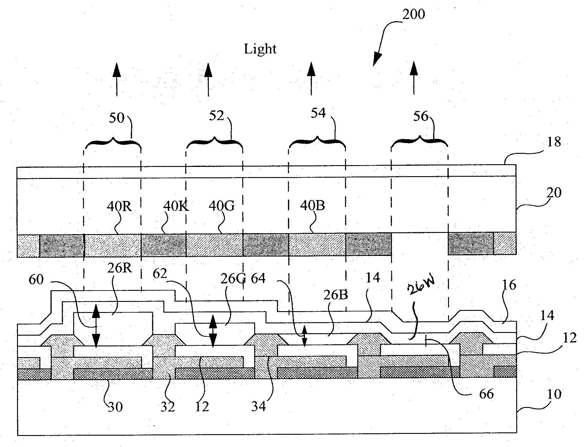
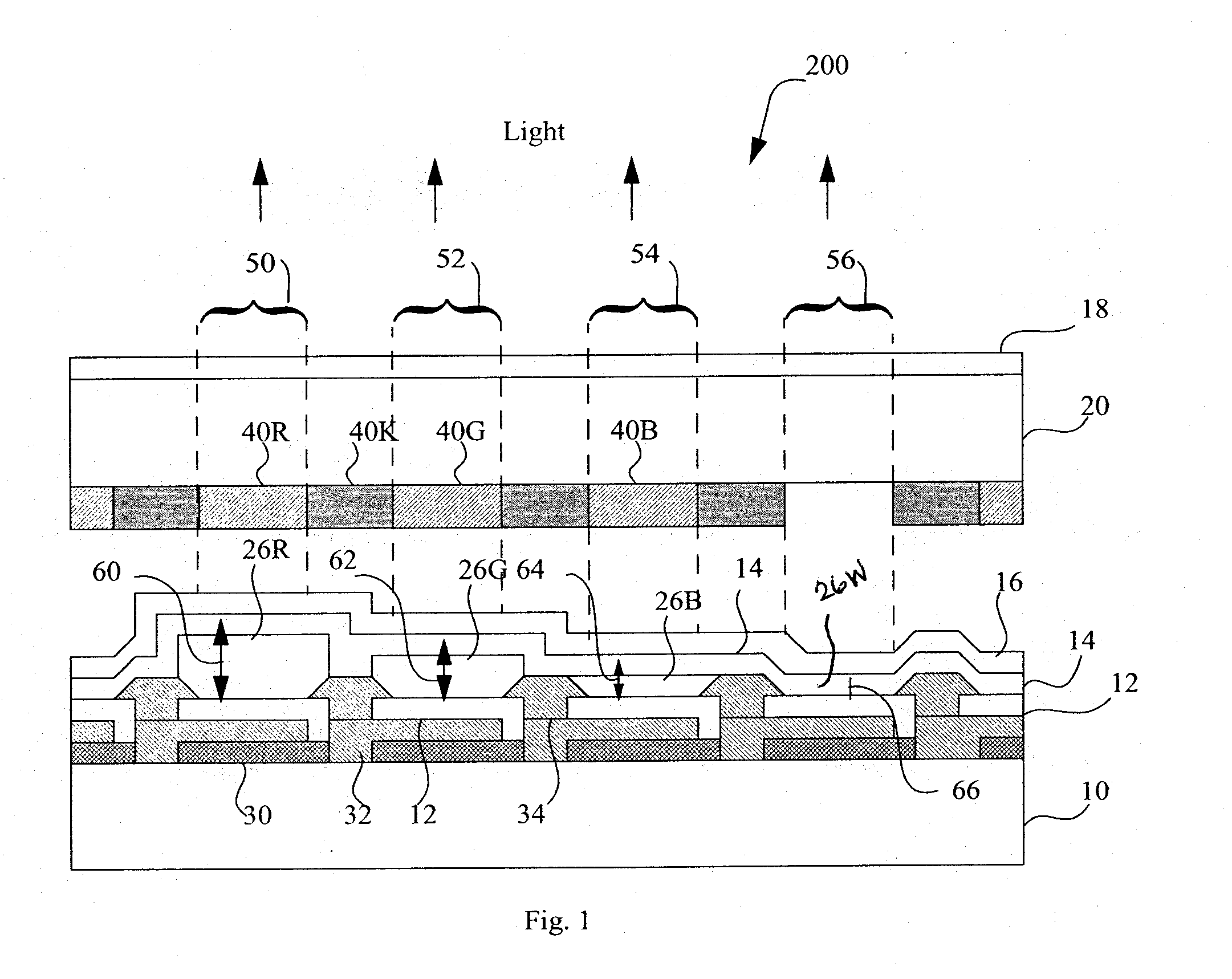
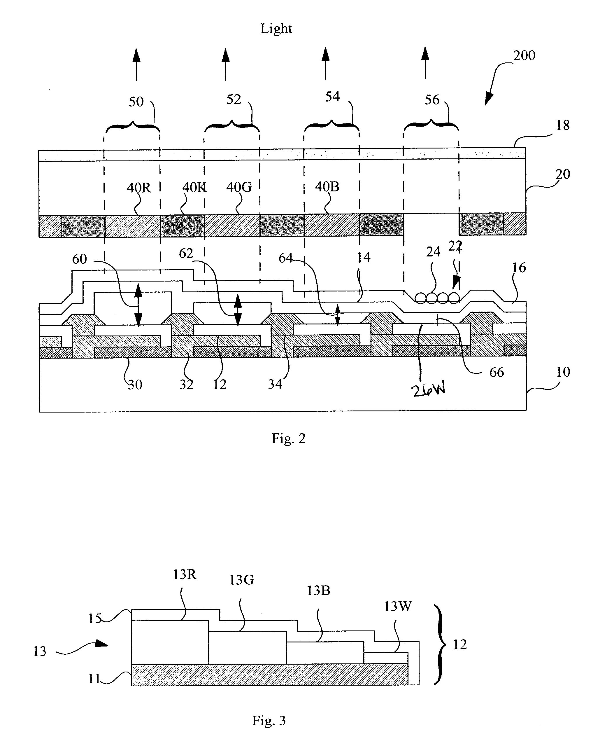
[0024]Referring to FIG. 1, a light-emitting diode device according to an embodiment of the present invention comprises a substrate 10, a reflective electrode 12, and a semi-transparent electrode 16 formed over the substrate 10. Either the reflective electrodes 12 or semi-transparent electrodes 16 is patterned to form a plurality of independently controllable light-emitting elements 50, 52, 54, and 56. The independently controllable light-emitting elements are controlled, for example by thin-film electronic components 30 formed on the substrate 10. The other electrode may be unpatterned and electrically common to all of the light-emitting elements. An unpatterned white light-emitting layer 14 is formed between the reflective electrode 12 and the semi-transparent electrode 16. Reflective electrode 12, semi-transparent electrode 16, and unpatterned white-light-emitting layer 14 form optical microcavities 60, 62, 64, and 66. A plurality of color filters 40R, 40G, and 40B are formed over...


PUM


Abstract

A light-emitting diode device, including a substrate; and a reflective electrode and a semi-transparent electrode formed over the substrate and an unpatterned white light-emitting layer formed between the reflective electrode and the semi-transparent electrode, the reflective electrode, semi-transparent electrode, and unpatterned white-light-emitting layer forming an optical microcavity, and wherein either the reflective or semi-transparent electrodes is patterned to form a plurality of independently controllable light-emitting elements with at least one light-emitting element having no color filter. Color filters are formed over a side of the semi-transparent electrodes opposite the unpatterned white light-emitting layer in correspondence with the light-emitting elements, the color filters having at least two different colors. Additionally, a reflected-light absorbing layer is located over all of the light-emitting elements.

Description

FIELD OF THE INVENTION[0001]The present invention relates to light-emitting diode (LED) devices, and more particularly, to LED device structures for improving light output and ambient contrast.BACKGROUND OF THE INVENTION[0002]Emissive flat-panel display devices are widely used in conjunction with computing devices and in particular with portable devices. These displays are often used in public areas with significant ambient illumination.[0003]Organic light emitting diodes (OLED) have many advantages in a flat-panel display device and are useful in optical systems. U.S. Pat. No. 6,384,529 issued May 7, 2002 to Tang et al. shows an OLED color display that includes an array of OLED light emitting elements (pixels). Light is emitted from a pixel when a current is passed through an organic material, the frequency of the light depending on the nature of the organic material that is used. The organic materials are placed upon a substrate between electrodes, with an encapsulating cover laye...

Claims


Application Information

Patent Timeline
Patent Type & Authority Applications(United States)
IPC IPC(8): H01L27/32H01J9/00
CPCH01L27/3213H01L27/322H01L51/5281H01L51/5268H01L51/5265H10K59/351H10K59/38H10K50/852H10K50/854H10K50/86
Inventor COK, RONALD S.TYAN, YUAN-SHENGSHORE, JOEL D.PREUSS, DONALD R.
Owner GLOBAL OLED TECH
Why Eureka
Try Eureka