
Pattern shape evaluation method, pattern shape evaluation device, pattern shape evaluating data generation device and semiconductor shape evaluation system using the same

a technology of data generation device and pattern shape, applied in image analysis, instruments, computing, etc., can solve problems such as difficult correlation, and time-consuming search edges, so as to reduce erroneous judgment of normal pattern area, simplify process sequence, and reduce the effect of erroneous detection of normal pattern area

Active Publication Date: 2009-02-26
HITACHI HIGH-TECH CORP
View PDF9 Cites 37 Cited by
  • Summary
  • Abstract
  • Description
  • Claims
  • Application Information

AI Technical Summary

Benefits of technology

[0008]In view of these issues, the present invention provides a pattern shape evaluation method capable of reducing erroneous judgments of normal pattern areas which have been the problems of conventional techniques, and detecting a pattern defect position at high speed by simplifying the process sequence, a pattern shape evaluation device, a pattern shape evaluation data generation device, and a semiconductor shape evaluation system using the same.
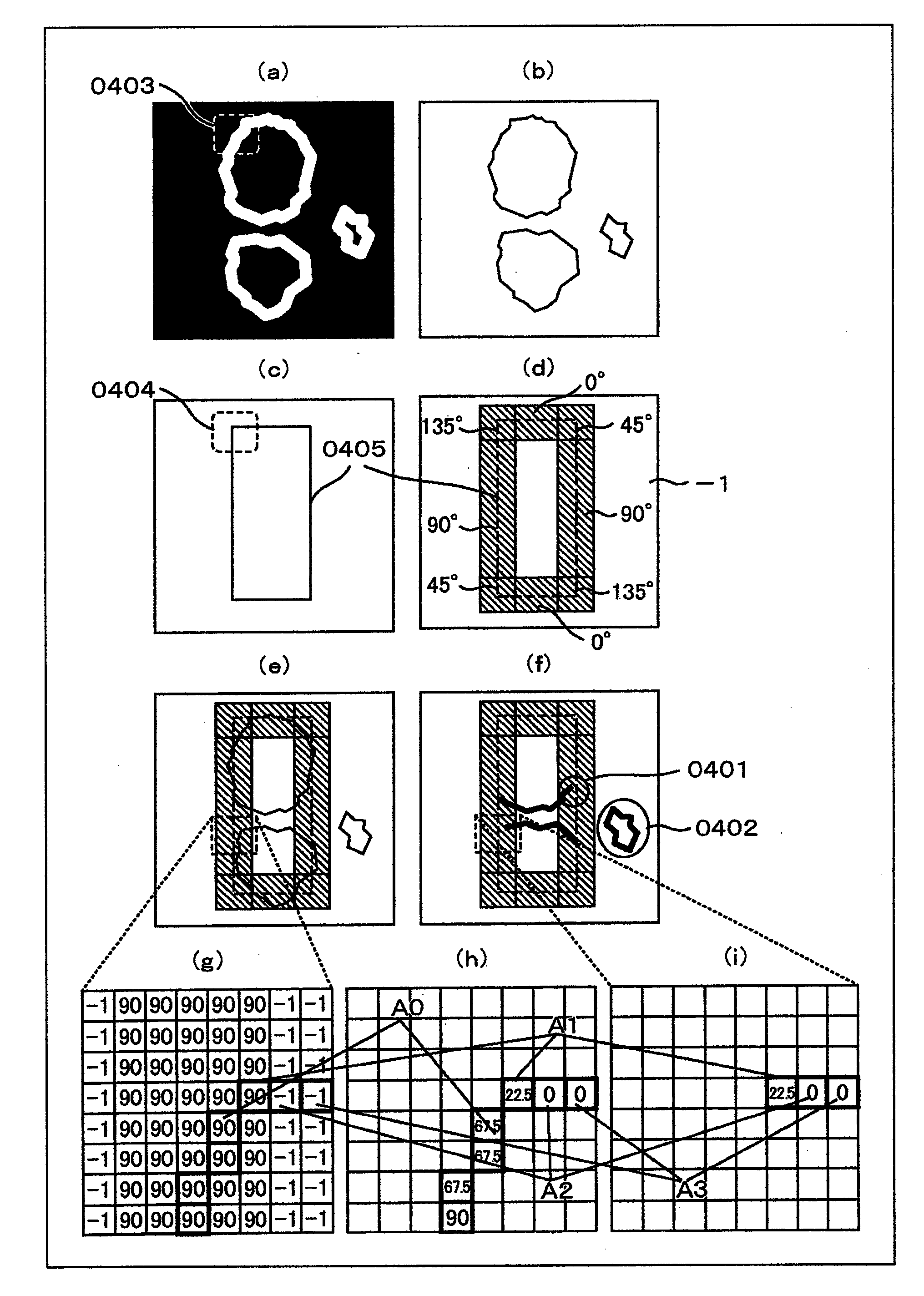
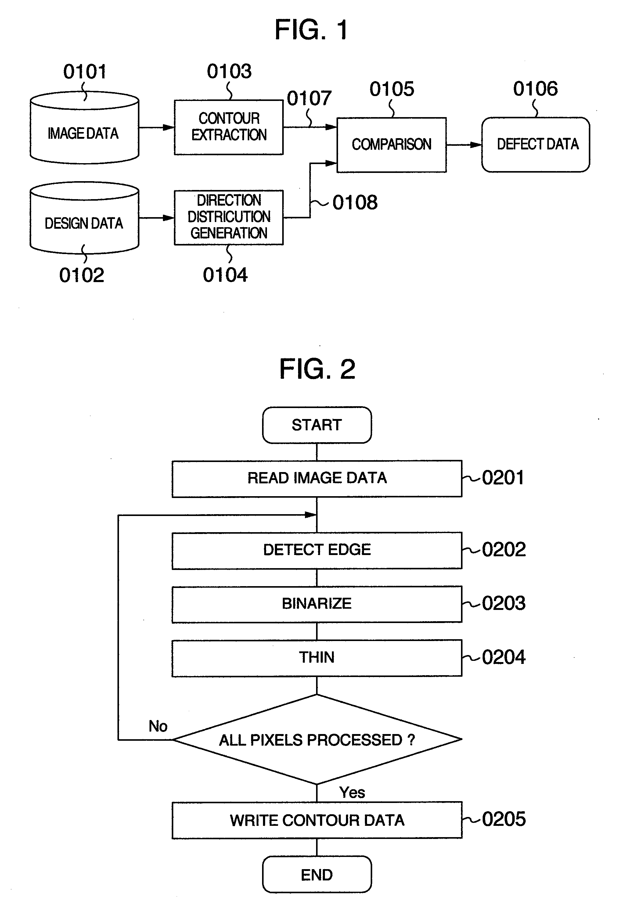
[0030]As described above, according to the present invention, it is possible to reduce erroneous judgments of normal pattern areas which have been the problems of conventional techniques and to detect a pattern defect position at high speed by simplifying the process sequence, through comparison between contour data extracted from image data and direction distribution data representative of a pattern direction and tolerance range using design data as a criterion.

Problems solved by technology

With this method of searching edges of the inspection object pattern in one direction using each edge of the design pattern as a judgment criterion, however, if a pattern shape is deformed more or less relative to the design data, a pattern area may exist which is difficult to be correlated to the design data, resulting in a problem of erroneously detecting a normal pattern area as a defect.
Further, if a correlating direction range is broadened, it takes a time to search edges.

Method used


Image

  • Pattern shape evaluation method, pattern shape evaluation device, pattern shape evaluating data generation device and semiconductor shape evaluation system using the same
  • Pattern shape evaluation method, pattern shape evaluation device, pattern shape evaluating data generation device and semiconductor shape evaluation system using the same
  • Pattern shape evaluation method, pattern shape evaluation device, pattern shape evaluating data generation device and semiconductor shape evaluation system using the same

Examples


first embodiment

(1) First Embodiment

[0071]FIG. 1 is a block diagram illustrating a basic principle of the present invention. FIG. 4 is a diagram showing data to be used in each block shown in FIG. 1.

[0072]The present invention is reduced in practice by a computer system such as shown in FIG. 5. Connected to a system bus 0507 of the computer system are a central processing unit (CPU) 0501, a memory 0502, an input / output (I / O) controller 0505, a network interface 0508 and a frame memory 0510. The I / O controller 0505 connects a disc 0506 storing design data of semiconductor and a photographed image of semiconductor, and receives from an external a signal such as parameters to be used for inspection of the present invention via a data input unit such as a mouse 0503 and a keyboard 0504. The frame memory 0510 stores therein data to be displayed on a display 0511, such as photographed images and design data of semiconductor and results of pattern shape evaluation of the present invention. The system bus ...

second embodiment

(2) Second Embodiment

[0100]This embodiment describes a method of inspecting an abnormal state and a defect of a pattern by utilizing direction distribution data 0108 defined by a user. This invention is also reduced in practice by the computer system shown in FIG. 5. Processes other than those of the direction distribution generation unit 0104 are similar to those of the first embodiment, and the description thereof is omitted.

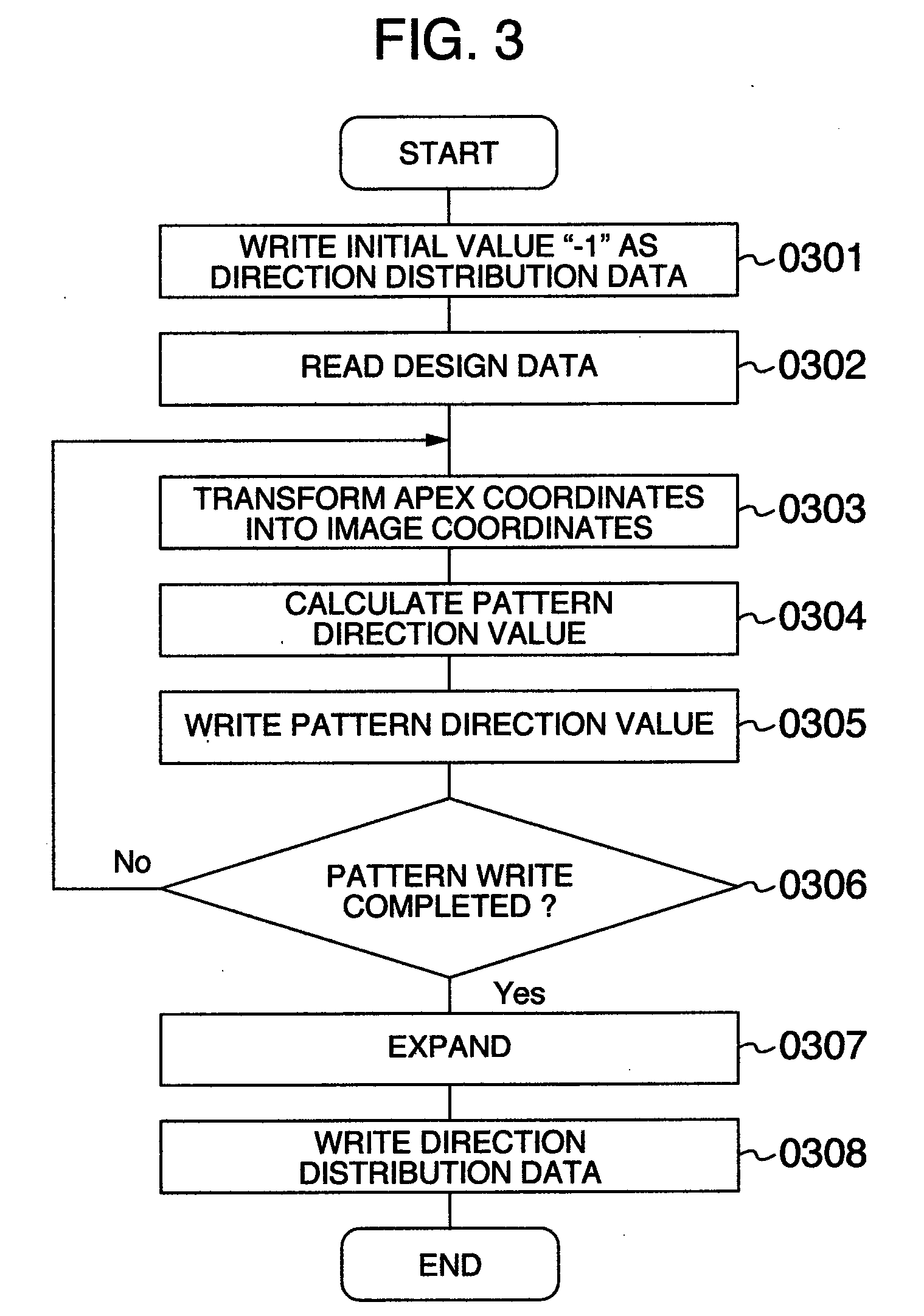
[0101]FIG. 14 is a flow chart illustrating the process to be executed by the direction distribution generation unit 0104 of the present invention. The design data 0102 is first read at Step 1401, direction distribution data 0108 is generated by a simplified method described in the first embodiment at Step 1402, and thereafter the direction distribution data 0108 is written in the frame memory and displayed on the display at Step 1403. Next, a user is urged to input a correction value of the direction distribution data 0108 via the keyboard or mouse. In accorda...

third embodiment

(3) Third Embodiment

[0102]This embodiment shows a method of inspecting an abnormal state and a defect of a pattern by utilizing parameters designated by a user for generating direction distribution data 0108 and efficiently generating the direction distribution data 0108. This invention is also reduced in practice by the computer system shown in FIG. 5. Processes other than those of the direction distribution generation unit 0104 are similar to those of the first embodiment, and the description thereof is omitted.

[0103]FIG. 16 is a flow chart illustrating a generation sequence for direction distribution data.

[0104]First, a parameter input screen for generating the direction distribution data 0108 is displayed on the display at Step 1601. As shown in FIG. 15A, the display also displays data allowing a user to judge the relation among respective parameters, design data 1501 and a tolerance area 1502. Examples of a parameter to be designated by a user are shown below.

[0105](1) H: a par...


PUM


Abstract

A pattern shape evaluation method and semiconductor inspection system having a unit for extracting contour data of a pattern from an image obtained by photographing a semiconductor pattern, a unit for generating pattern direction data from design data of the semiconductor pattern, and a unit for detecting a defect of a pattern, through comparison between pattern direction data obtained from the contour data and pattern direction data generated from the design data corresponding to a pattern position of the contour data.

Description

BACKGROUND OF THE INVENTION[0001]1. Field of the Invention[0002]The present invention relates to a pattern shape evaluation method of inspecting a pattern formed on a photomask or wafer by using an image obtained by photographing a semiconductor device and design data of the semiconductor device, a pattern shape evaluation device, and a semiconductor inspection system using the method and device.[0003]2. Description of the Related Art[0004]In recent years, there have been situations where manufacture of semiconductor devices is difficult because of minituarization and multilayering thereof have been progressed and because logic thereof has been more complicated. As a result, there has been a tendency that defects to be attributed to manufacturing processes occur frequently, and it has been important to detect detects efficiently and accurately and identify problems of manufacturing processes.[0005]The defects to be attributed to manufacturing processes include a deformed pattern, a ...

Claims


Application Information

Patent Timeline
Patent Type & Authority Applications(United States)
IPC IPC(8): G06K9/00G06V10/44
CPCG06K9/00G06F17/5081G06T7/0004G06K2209/19G06V2201/06G06V10/44G06V10/993G06F30/398
Inventor TOYODA, YASUTAKAMATSUOKA, RYOICHISUGIYAMA, AKIYUKI
Owner HITACHI HIGH-TECH CORP
Learn More