Semiconductor Chip with Stratified Underfill

a technology of semiconductors and underfills, applied in semiconductor devices, semiconductor/solid-state device details, electrical apparatus, etc., can solve the problems of imposing tremendous stress on solder bumps, bump failure and delamination, and penalizing disparate materials

Active Publication Date: 2009-03-05
INNOVATIVE FOUNDRY TECH LLC
View PDF20 Cites 23 Cited by
  • Summary
  • Abstract
  • Description
  • Claims
  • Application Information

AI Technical Summary

Problems solved by technology

Although these various materials provide certain favorable characteristics, there is a penalty for using disparate materials.
The differences in CTE between a semiconductor chip and the package substrate can, if not compensated for, impose tremendous stresses on the solder bumps.
If the stresses are too large, bump failure and delamination can occur.
Unfortunately, the conventional underfill material may still present a rather abrupt difference in CTE relative to both the chip and the substrate.

Method used


Image

  • Semiconductor Chip with Stratified Underfill
  • Semiconductor Chip with Stratified Underfill
  • Semiconductor Chip with Stratified Underfill

Examples


Embodiment Construction

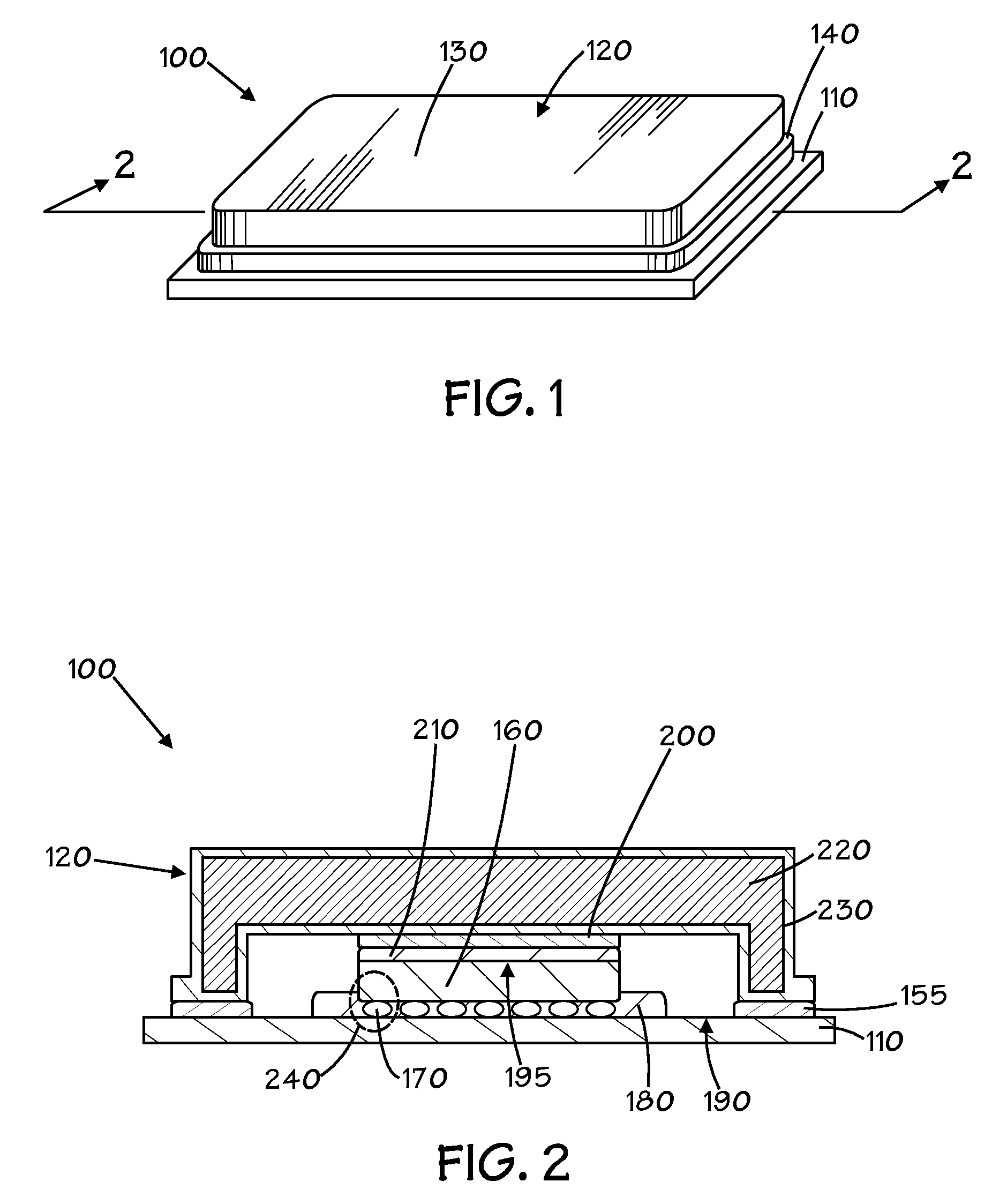
[0023]In the drawings described below, reference numerals are generally repeated where identical elements appear in more than one figure. Turning now to the drawings, and in particular to FIG. 1, therein is shown a pictorial view of an exemplary embodiment of a semiconductor chip package 100 that includes a base substrate 110 and a lid 120 seated thereon. The lid 120 is depicted as a top hat design that includes a crown portion 130 and a brim or flange portion 140. However it should be understood that the lid 120 may be configured as a standard bathtub design or other type of lid. Indeed, the lid 120 may be omitted entirely if a lidless design is desired. The substrate 110 is advantageously an organic substrate that may be standard core, thin core or coreless as desired.

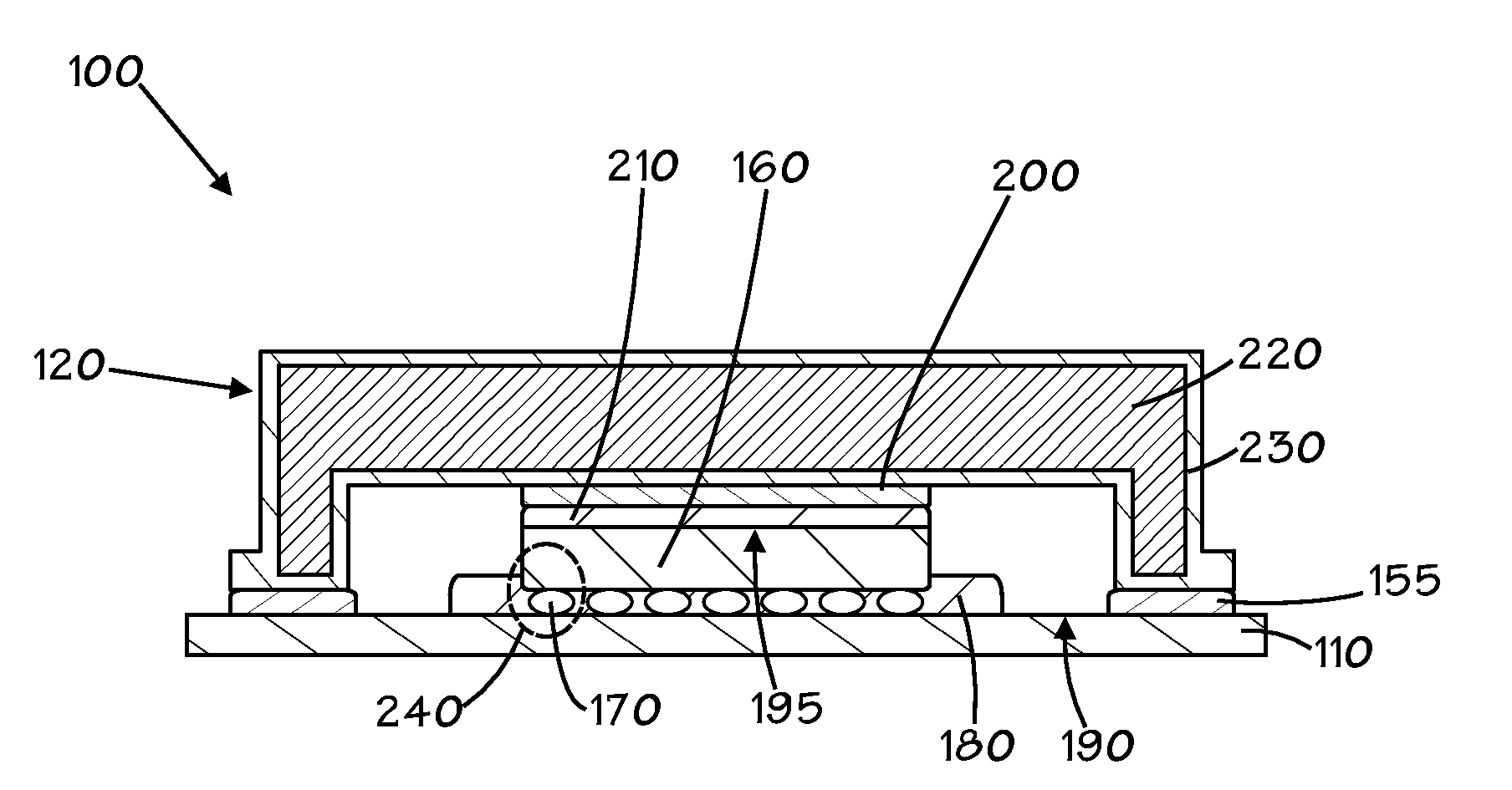
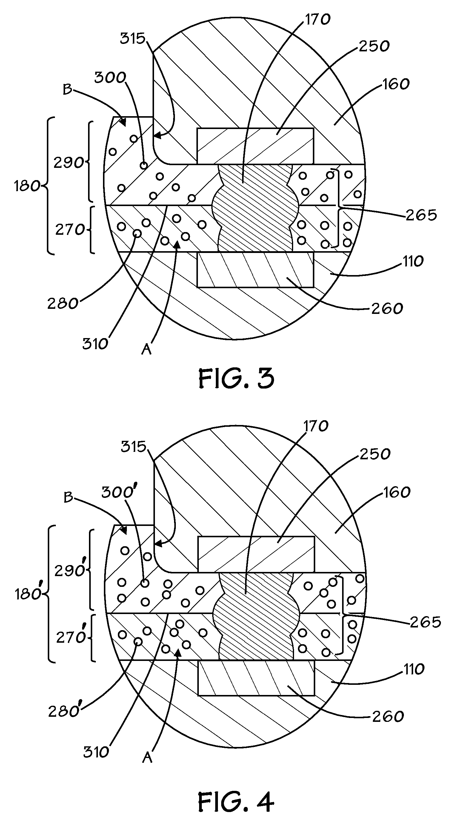
[0024]Additional detail regarding the semiconductor chip package 100 may be understood by referring now also to FIG. 2, which is a sectional view of FIG. 1 taken at 2-2. The substrate 110 may be configured as a pin g...


PUM

PropertyMeasurementUnit
sizeaaaaaaaaaa
sizeaaaaaaaaaa
bulk modulusaaaaaaaaaa

Abstract

Various semiconductor chip underfills and methods of making the same are provided. In one aspect, a method of manufacturing is provided that includes coupling a semiconductor chip to a substrate to leave a gap therebetween, and forming an underfill layer in the gap. The underfill layer includes a first plurality of filler particles that have a first average size and a second plurality of filler particles that have a second average size smaller than the first average size such that the first plurality of filler particles is concentrated proximate the substrate and the second plurality of filler particles is concentrated proximate the semiconductor chip so that a bulk modulus of the underfill layer is larger proximate the substrate than proximate the semiconductor chip.

Description

BACKGROUND OF THE INVENTION[0001]1. Field of the Invention[0002]This invention relates generally to semiconductor processing, and more particularly to semiconductor chip underfills and methods of making the same.[0003]2. Description of the Related Art[0004]Many types of conventional packaged integrated circuits consist of a semiconductor chip flip-chip mounted to a package substrate. Electrical interconnections between the semiconductor chip and a package substrate are provided by a plurality of solder bumps. The materials used for the semiconductor chip, the solder bumps, and the package substrate are selected for certain desirable characteristics. For example, the semiconductor chip is usually composed of silicon or a laminate of silicon and silicon dioxide. Silicon is selected for its advantageous semiconductor properties. Solder is selected as a bump material due to its electrical conductivity and easy thermal reflow properties. Conventional organic package substrates are freque...

Claims


Application Information

Patent Timeline
Patent Type & Authority Applications(United States)
IPC IPC(8): H01L23/18H01L21/56
CPCH01L21/563H01L23/053H01L2224/32225H01L2224/16225H01L2924/1433H01L23/3164H01L2224/73203H01L2224/73204H01L2224/73253H01L2924/01078H01L2924/01079H01L2924/12044H01L2924/00H01L2224/05571H01L2224/05573H01L2224/05639H01L2224/05644H01L2224/05655H01L2224/05669H01L24/05
Inventor ZHAI, JUNGANNAMANI, RANJITPARTHASARATHY, SRINIVASAN
Owner INNOVATIVE FOUNDRY TECH LLC
Why Eureka
Try Eureka