High-sensitive resistance measuring device and monitoring method of solder bump

a resistance measurement and resistance measurement technology, applied in the direction of resistance/reactance/impedence, individual semiconductor device testing, instruments, etc., can solve the problems of increasing the stress distortion of the solder bump connection unit, minute cracks in the solder bump of the bga package, and damage such as minute cracks, etc., to achieve the effect of causing damag

Inactive Publication Date: 2009-03-05
FUJITSU LTD
View PDF3 Cites 39 Cited by
  • Summary
  • Abstract
  • Description
  • Claims
  • Application Information

AI Technical Summary

Problems solved by technology

When the size of the BGA package is increased in this manner, due to mutual difference in thermal expansion coefficients caused by thermal cycles of the system board, the BGA package, and semiconductor ICs constituting processors having different materials, stress is repeatedly applied to the solder connection units between solder bumps of the BOA package and the circuit board, and there is a danger that stress distortions of the solder bump connection units are increased, thereby causing damages such as minute cracks.
The size of the circuit board such as a system board on which BGA packages are mounted has also been increased; and, when the size of the circuit board is increased, there is a danger that board deformation caused during handling or board assembly processes of the circuit board may cause damages such as minute cracks in solder bumps of the BGA package.
When the minute cracks are generated in the solder bumps of the BGA package, the cracks gradually grow along with time elapse; and, when the development state of the cracks exceeds a certain limitation, the cracks rapidly grow, thereby rapidly increasing the resistance of the solder bumps and sometimes leading to rupture, and these damages such as the minute cracks are a cause of long-term reliability deterioration.
The damages of the solder bumps in the BGA package cause increase of the resistance of the solder bump connection units; however, in order to detect initial damages of minute crack generation, extremely minute resistance variations have to be detected.
However, detection of resistance variations of the solder bump connection unit using such a conventional four-terminal method has a problem that the detection sensitivity is insufficient, and minute resistance variations cannot be accurately detected.
However, since the initial resistance of the solder bump is 1 ohm, the initial value of the measured voltage is 100 mill volts, which is the max of the range; and, when the resistance thereafter is increased by 0.01 ohm, the measured voltage overflows to 101 mill volts, and minute resistance variations cannot be measured, which is a problem.
Furthermore, when a particular solder bump connection unit is subjected to quality determination by detecting minute resistance variations, since the resistance is varied also by the temperature variations of the entire package, the resistance variation caused by damages such as cracks of the solder bump connection unit and the resistance variation caused by the temperature variation cannot be distinguished from each other, and the resistance variation caused by the damages of the solder bump connection unit cannot be detected, which is a problem.

Method used


Image

  • High-sensitive resistance measuring device and monitoring method of solder bump
  • High-sensitive resistance measuring device and monitoring method of solder bump
  • High-sensitive resistance measuring device and monitoring method of solder bump

Examples


Embodiment Construction

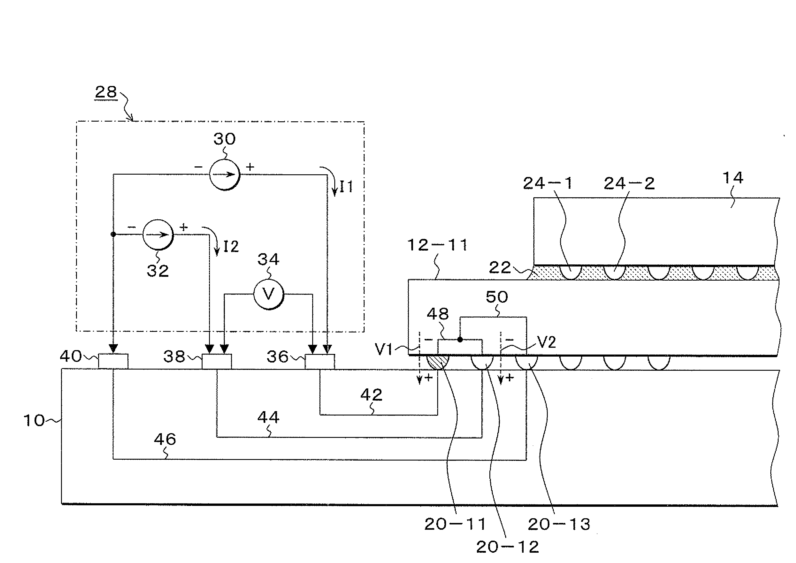
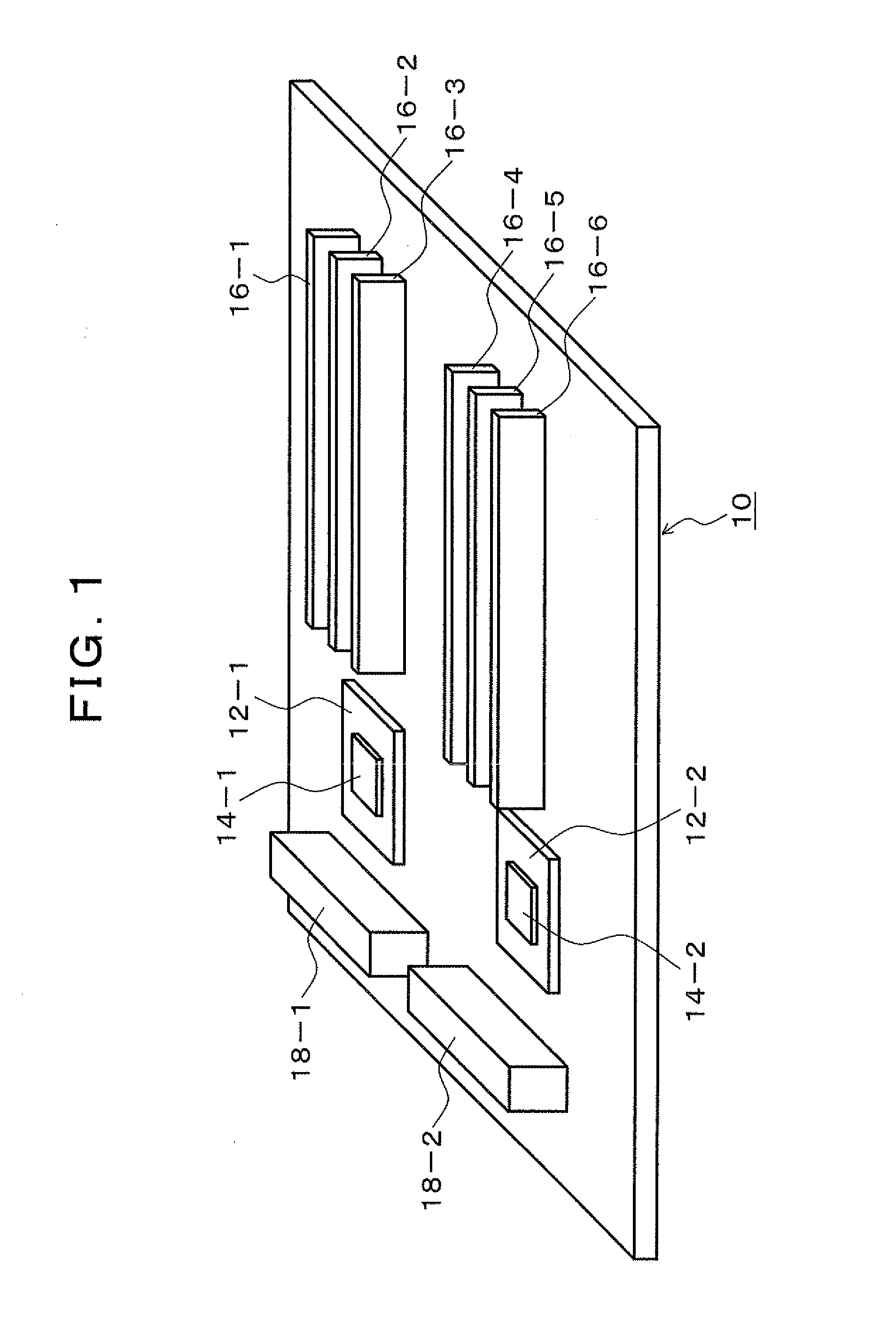
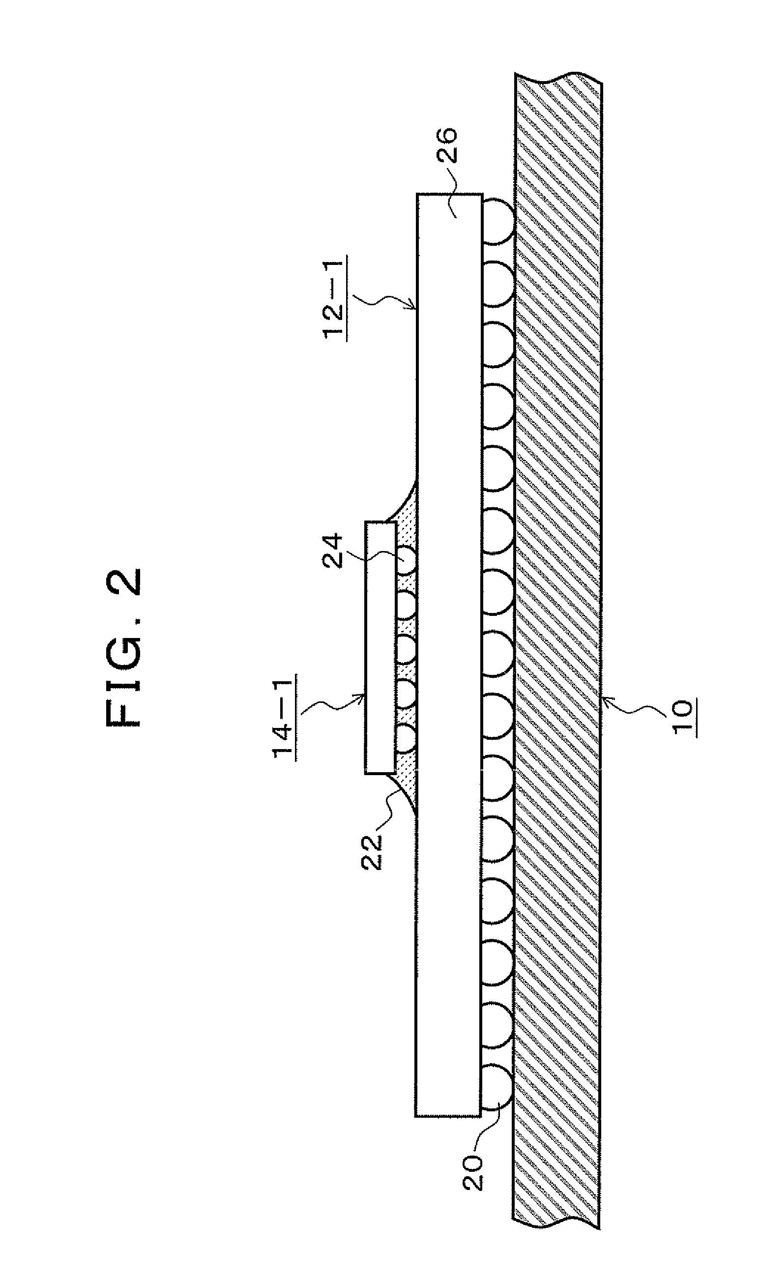
[0024]FIG. 1 is an explanatory drawing showing a mother board on which BGA packages serving as resistance measurement objects according to the present art are mounted. In FIG. 1, the mother board 10 is, for example, a circuit board incorporated in a chassis or the like of a server, the BGA packages 12-1 and 12-2 are mounted on the mother board, and, for example, processor modules 14-1 and 14-2 are mounted as LSIs on the BGA packages 12-1 and 12-2 in this embodiment. In addition, on the mother board 10, semiconductor parts such as memory modules 16-1 to 16-6 and power source modules 18-1 and 18-2 are mounted. Regarding the mother board 10 used by incorporating in a server chassis, recently, the board size is a large size, for example, exceeding several tens of centimeters by several tens of centimeters; and, there are high possibilities that flexure or deformation is generated in the entire board in handling or assembly processes of the mother board 10 since the size is large, thereb...


PUM


Abstract

According to an aspect of an embodiment, a high-sensitive resistance measuring device of solder bumps comprises a resistance variation detection unit which detects a differential voltage (□V=V1−V2), which is obtained by subtracting a second voltage (V2) generated in a reference bump connection unit by a constant current (I) from a second constant current source from a first voltage (V1) generated in a monitored bump connection unit by the constant current I from a first constant current source, as a resistance variation voltage representing a resistance variation (□R) of the monitored bump connection unit.

Description

[0001]This application is a priority based on prior applications No. JP 2007-219993, filed Aug. 23, 2007, in Japan.BACKGROUND[0002]1. Field[0003]The present art relates to a high-sensitive resistance measuring device and method of solder bumps which monitor the solder connection state of a package such as a ball grid array mounted on a circuit board by the solder bumps and, particularly, relates to the high-sensitive resistance measuring device and monitoring method of the solder bumps which detect and monitor minute variations of resistance caused by cracks generated in the solder bumps by stress.[0004]2. Description of the Related Arts[0005]Recently, in a ball grid array package (hereinafter, referred to as a “BGA package”) that mounts plural processors on a system board of, for example, a server, power source pins and signal pins are increased to 1000 pins or 2000 pins due to enhancement of functions and increase of power consumption of the server, and the size of the BGA package...

Claims


Application Information

Patent Timeline
Patent Type & Authority Applications(United States)
IPC IPC(8): G01R31/26
CPCG01R27/14G01R31/048H01L2224/16225H01L2224/32225H01L2224/73204H01L2924/15311H01L2924/00G01R31/71
Inventor NAKAMURA, NAOAKI
Owner FUJITSU LTD
Why Eureka
Try Eureka