Semiconductor memory device and method for driving the same

a technology of memory device and semiconductor, which is applied in the direction of pulse manipulation, pulse technique, instruments, etc., can solve the problems of increasing data input/output speed of semiconductor and synchronous memory device not keeping up with data processor operating speed

Active Publication Date: 2009-03-05
SK HYNIX INC
View PDF18 Cites 32 Cited by
  • Summary
  • Abstract
  • Description
  • Claims
  • Application Information

AI Technical Summary

Benefits of technology

[0011]Embodiments of the present invention are directed to providing a duty cycle correction circuit of a semiconductor device, which can output a duty cycle corrected clock and its inverted clock having substantially exactly 180° phase difference therebetween.

Problems solved by technology

As semiconductor integrated circuit (IC) technologies are rapidly developed, the operating speed of the data processor increases, but the data input / output speed of the semiconductor memory device does not keep up with the increasing operating speed of the data processor.
However, even the synchronous memory device could not keep up with the operating speed of the data processor, and thus a double data rate (DDR) synchronous memory device was developed.
As the frequency of the system clock is increasing, the deficient operation processing margin at one of the rising and falling edges means that it is difficult to process data stably.
During this process, however, the phase difference between the clock and the inverted clock may not become 180°, that is, their phases are distorted.
In this case, if the semiconductor memory device operates using the clocks outputted from the duty cycle correction circuit, it cannot perform the predefined operations at each transition of the system clock.

Method used


Image

  • Semiconductor memory device and method for driving the same
  • Semiconductor memory device and method for driving the same
  • Semiconductor memory device and method for driving the same

Examples


Embodiment Construction

[0025]Hereinafter, a semiconductor memory device and a method for driving the same in accordance with the present invention will be described in detail with reference to the accompanying drawings.

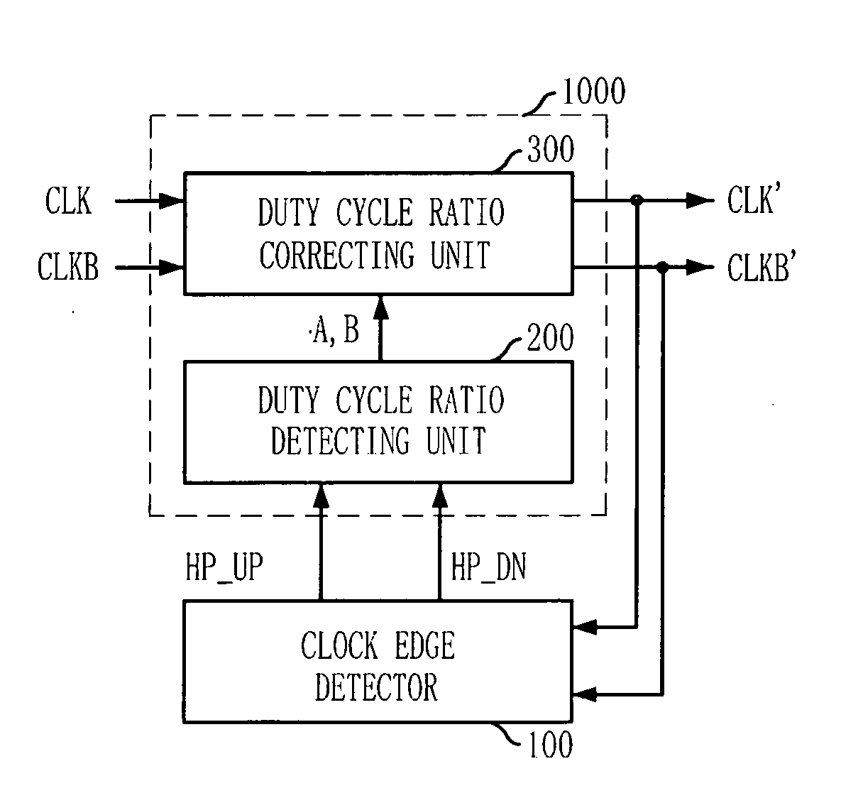
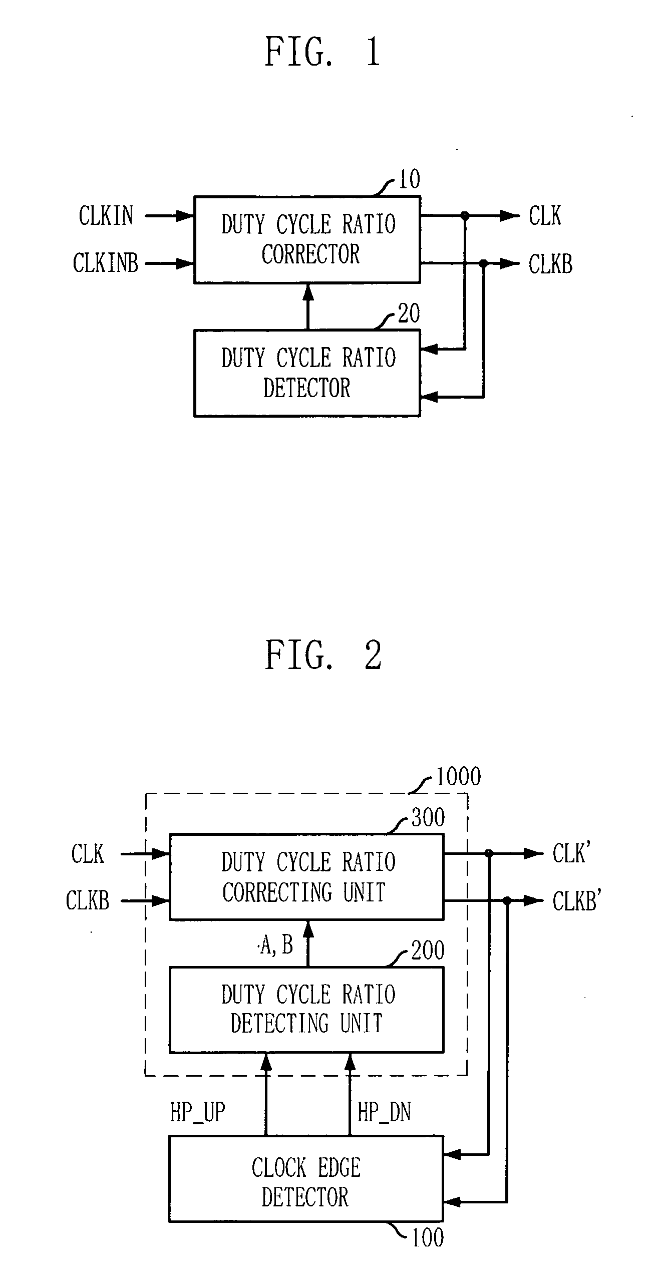
[0026]FIG. 1 is a block diagram of a duty cycle correction circuit of a semiconductor device.

[0027]Referring to FIG. 1, the duty cycle correction circuit includes a duty cycle ratio corrector 10 and a duty cycle ratio detector 20.

[0028]The duty cycle ratio corrector 10 corrects duty cycle ratios of a first clock CLKIN and a second clock CLKINB to output duty cycle-corrected clocks CLK and CLKB. The duty cycle ratio detector 10 detects distortion degree between the duty cycle ratios of the clocks CLK and CLKB and controls the duty cycle ratio correct 10 to correct the duty cycle ratios of the clocks CLK and CLKB.

[0029]Since the DDR2 synchronous memory device outputs data at both rising and falling edges, it is very important to correct the duty cycle ratio of the system clock. Semiconductor ...


PUM


Abstract

A semiconductor memory device has a duty cycle correction circuit capable of outputting a duty cycle corrected clock and its inverted clock having substantially exactly 180° phase difference therebetween. The semiconductor memory device includes a duty cycle corrector configured to receive a first clock and a second clock to generate a first output clock and a second output clock whose duty cycle ratios are corrected in response to correction signals, and a clock edge detector configured to generate the correction signals corresponding to an interval between a reference transition timing of the first output clock and a reference transition timing of the second output clock.

Description

CROSS-REFERENCE TO RELATED APPLICATIONS[0001]The present invention claims priority to Korean patent application number 10-2007-0089521, filed on Sep. 4, 2007, which is incorporated by reference in its entirety.BACKGROUND OF THE INVENTION[0002]The present invention relates to a semiconductor integrated circuit, and more particularly to a duty cycle correction circuit of a semiconductor integrated circuit.[0003]In a system including a variety of semiconductor devices having various functions, a semiconductor memory device serves as a data storage. The semiconductor memory device outputs data corresponding to addresses received from a data processor, e.g., a central processing unit (CPU), or stores data received from the data processor into unit cells corresponding to addresses inputted together with the data.[0004]As the operating speed of the system is increasing, the data processor requires the semiconductor memory device to input / output data at higher speed. As semiconductor integr...

Claims


Application Information

Patent Timeline
Patent Type & Authority Applications(United States)
IPC IPC(8): H03K3/017
CPCH03K5/1565H03K5/1534G11C11/407G11C11/4076
Inventor KIM, KYUNG-HOONLEE, JUN-WOOSONG, TAEK-SANG
Owner SK HYNIX INC
Why Eureka
Try Eureka