Imaging apparatus and method for driving solid-state imaging device

Inactive Publication Date: 2009-03-05
FUJIFILM CORP
View PDF1 Cites 4 Cited by
  • Summary
  • Abstract
  • Description
  • Claims
  • Application Information

AI Technical Summary

Benefits of technology

[0008]The invention has been made in view of the above circumstances and provides an imaging apparatus which is mounted with a solid-state imaging device that can concurrently obtain two types of imaging signals by controlling the exposure times for photoelectric conversion elements and which can reduce noise contained in the imaging signals.
[0017]With the above configuration, it is possible to provide an imaging apparatus which is mounted with a solid-state imaging device that can concurrently obtain two types of imaging signals by controlling the exposure times for photoelectric conversion elements and which can reduce noise contained in the imaging signals.

Problems solved by technology

When the thus generated electrons enter the photoelectric conversion elements, white defects would be caused.
As described above, if there is a difference between S / N of the signals obtained from the photoelectric conversion elements, the exposure time for which is long, and S / N of the signals obtained from the photoelectric conversion elements, the exposure time for which is short, due to the influence of the white defects, a quality of a wide dynamic range image, which is obtained by combining image data being generated from the both signals, is deteriorated.

Method used


Image

  • Imaging apparatus and method for driving solid-state imaging device
  • Imaging apparatus and method for driving solid-state imaging device
  • Imaging apparatus and method for driving solid-state imaging device

Examples


first embodiment

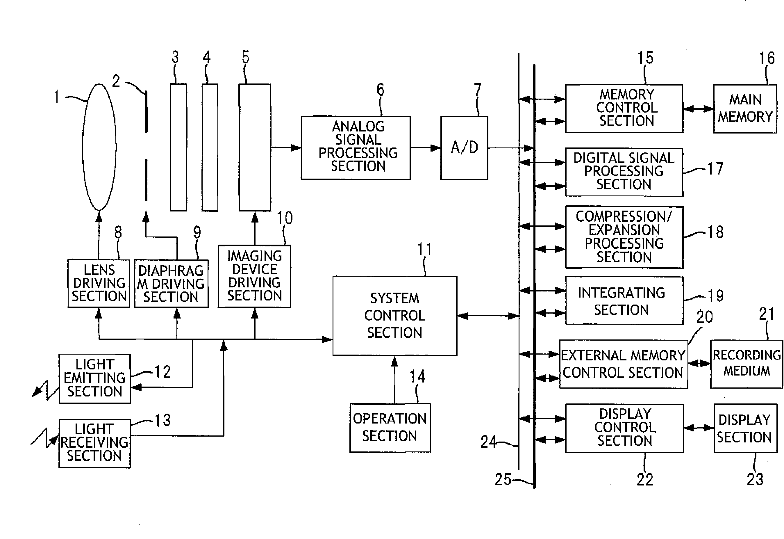
[0026]FIG. 1 is a view showing an outline of the configuration of a digital camera that is an example of an imaging apparatus with reference to which a first embodiment of the invention will be described.

[0027]A taking-image system of the digital camera shown in the figure includes a taking lens 1, a solid-state imaging device 5, an aperture diaphragm 2 which is arranged between the taking lens 1 and the solid-state imaging device 5, an infrared cut filter 3; and an optical low-pass filter 4.

[0028]A system control section 11 for controlling the entire electric controlling system of the digital camera controls a flash light emitting section 12 and a light receiving section 13. The system control section 11 also controls a lens driving section 8 so as to adjust a position of the taking lens 1 to a focusing position and to adjust zooming. Furthermore, the system control section 11 controls the aperture diaphragm 2 through a diaphragm driving section 9 so as to adjust an exposure amount...

second embodiment

[0063]The configuration of a digital camera explained according to a second embodiment is the same as that shown in FIG. 1 and therefore will be described with reference to FIGS. 1 and 2.

[0064]The photographing operation of the digital camera of this embodiment will be described below. FIG. 4 is a flow chart showing an operation executed at a time of photographing with the digital camera of the second embodiment.

[0065]When a shutter button provided in the operation section 14 is half-pressed (step S1), the system control section 11 performs the automatic exposure process (AE) (step S2) and the automatic focus adjustment process (AF) (step S3), and also measure a dynamic range necessary for photographing a photographic object (step S4). The system control section II determines an exposure time for the photoelectric conversion element 51R, 51G, 51B and an exposure time for the photoelectric conversion element 51r, 51g, 51b based on the measured dynamic range and controls the imaging d...

third embodiment

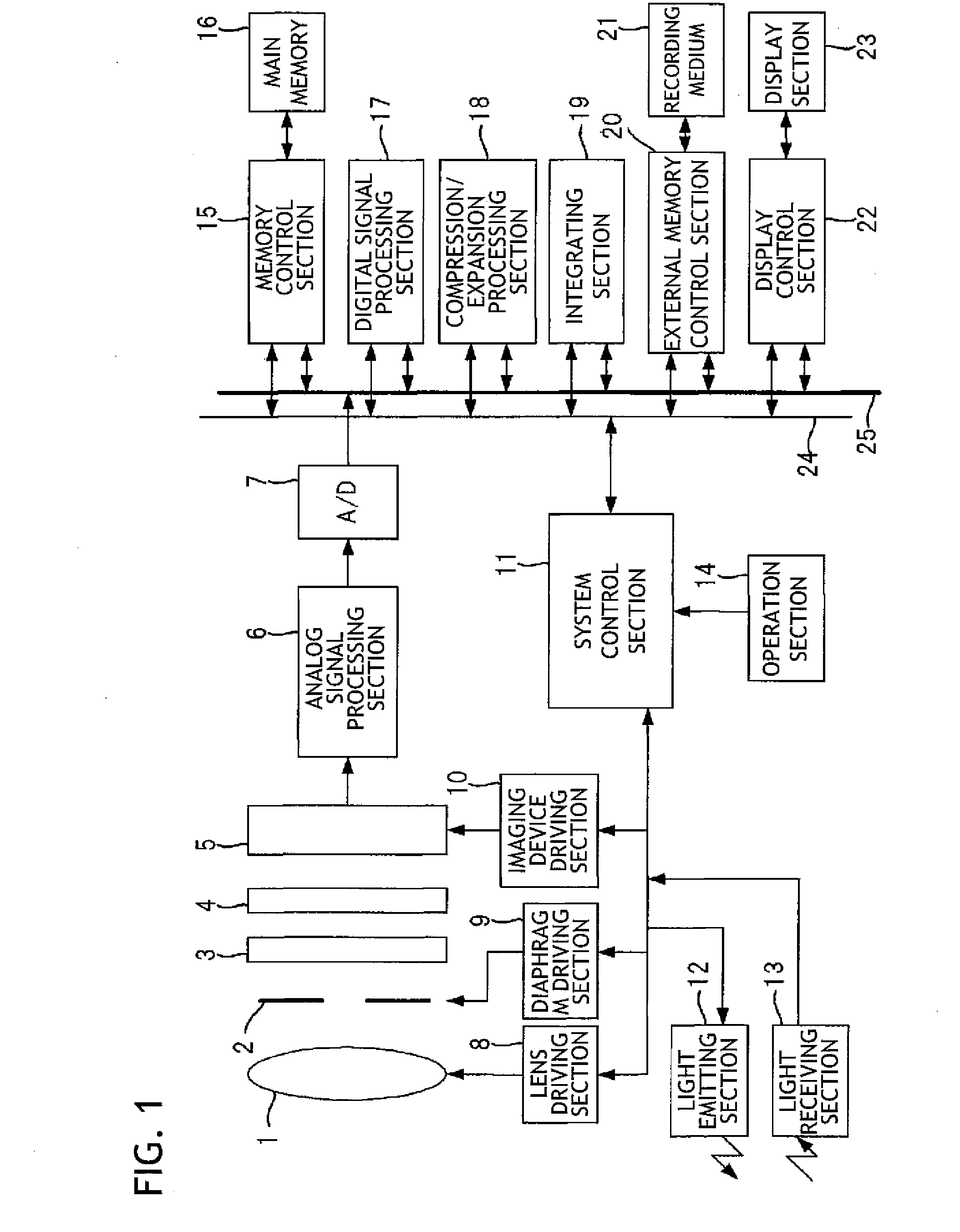
[0077]In the first and second embodiments, the photoelectric conversion elements of the solid-state imaging devices 5 are arranged in a so-called honeycomb arrangement in which an rgb group of photoelectric conversion elements and an rgb group of photoelectric conversion elements are shifted in the row direction X and the column direction Y by ½ of the arrangement pitch. However, the arrangement of the photoelectric conversion elements is not limited to this specific example. For example, the photoelectric conversion elements may be arranged in a square grid. In this embodiment, another configuration example of the solid-state imaging device will be described.

[0078]FIG. 6 is a schematic plan view showing another example of the configuration of the solid-state imaging devices mounted on the digital camera shown in FIG. 1.

[0079]A solid-state imaging device 5′ shown in FIG. 6 includes an RGB group of photoelectric conversion elements and an rgb group of photoelectric conversion element...


PUM


Abstract

A solid-state imaging device 5 includes photoelectric conversion elements 51R, 51G, 51B; and photoelectric conversion elements 51r, 51g, 51b. An exposure period for the photoelectric conversion elements 51r, 51g, 51b is controlled shorter than that for the photoelectric conversion elements 51R, 51G, 51B. During the exposure period for the photoelectric conversion elements 51R, 51G, 51B, an imaging device driving section 10 applies a readout pulse to transfer electrodes V2, V6, reads out electric charges accumulated in the photoelectric conversion elements 51r, 51g, 51b into vertical electric charge transfer paths 54, and controls to start exposure of the photoelectric conversion element 51r, 51g, 51b. During a period from start of the exposure of the photoelectric conversion elements 51R, 51G, 51B to the applying of the readout pulse, the imaging device driving section 10 applies a transfer pulse of a low level to the transfer electrodes V1 to V8.

Description

CROSS-REFERENCE TO RELATED APPLICATIONS[0001]This application is based upon and claims the benefit of priority from the Japanese Patent Application No. 2007-219892 filed on Aug. 27, 2007, the entire contents of which are incorporated herein by reference.BACKGROUND OF THE INVENTION[0002]1. Technical Field[0003]The invention relates to a solid-state imaging device and an imaging apparatus having a driving unit that drives the solid-state imaging device.[0004]2. Description of the Related Art[0005]In order to extend the dynamic range by obtaining low-sensitivity image data and high-sensitivity image data in a single photographing and combining them, there has been proposed a solid-state imaging device that includes photoelectric conversion elements having high sensitivity and photoelectric conversion elements having low sensitivity. In order to differentiate sensitivities among the photoelectric conversion elements, various methods are provided. For example, JP 2001-275044 A (correspon...

Claims


Application Information

Patent Timeline
IPC IPC(8): H04N5/335H01L27/148H04N5/341H04N5/353H04N5/357H04N5/369H04N5/3728
CPCH04N5/35554H04N5/3728H04N5/3594H04N25/583H04N25/623H04N25/73H01L27/146H04N25/42H04N25/60
Inventor KOBAYASHI, HIROKAZUNISHIDA, YOSHIYASU
Owner FUJIFILM CORP
Why Eureka
Try Eureka