Application of Multiple Voltage Droop Detection and Instruction Throttling Instances with Customized Thresholds Across a Semiconductor Chip

a technology of instruction throttling and voltage droop detection, which is applied in the direction of instruments, power supply for data processing, sustainable buildings, etc., can solve the problems of voltage dips (droops), limiting the speed of the circuit in the processor, and the noise condition due to the switching activity on the chip becoming a major new challeng

Inactive Publication Date: 2009-03-05
IBM CORP
View PDF28 Cites 37 Cited by
  • Summary
  • Abstract
  • Description
  • Claims
  • Application Information

AI Technical Summary

Problems solved by technology

As the trend of integrating more functions in a single high performance integrated circuit device (also called a chip) continues, the on-chip noise condition due to switching activity on the chip has become a major new challenge.
Power supply and power distribution system noise, especially voltage dips (droops) due to large step current increases, are a limiting factor in how fast the circuits in the processors can operate.
However, as design frequencies have risen over the years, decoupling capacitance is becoming either less effective at the frequencies that are required to have an effect, or are too costly in financial terms or power dissipation terms.
However, there are situations where the sensitivity to voltage droop of circuits in any given location on the chip may be greater or less than those in other areas of the chip.

Method used


Image

  • Application of Multiple Voltage Droop Detection and Instruction Throttling Instances with Customized Thresholds Across a Semiconductor Chip
  • Application of Multiple Voltage Droop Detection and Instruction Throttling Instances with Customized Thresholds Across a Semiconductor Chip
  • Application of Multiple Voltage Droop Detection and Instruction Throttling Instances with Customized Thresholds Across a Semiconductor Chip

Examples


Embodiment Construction

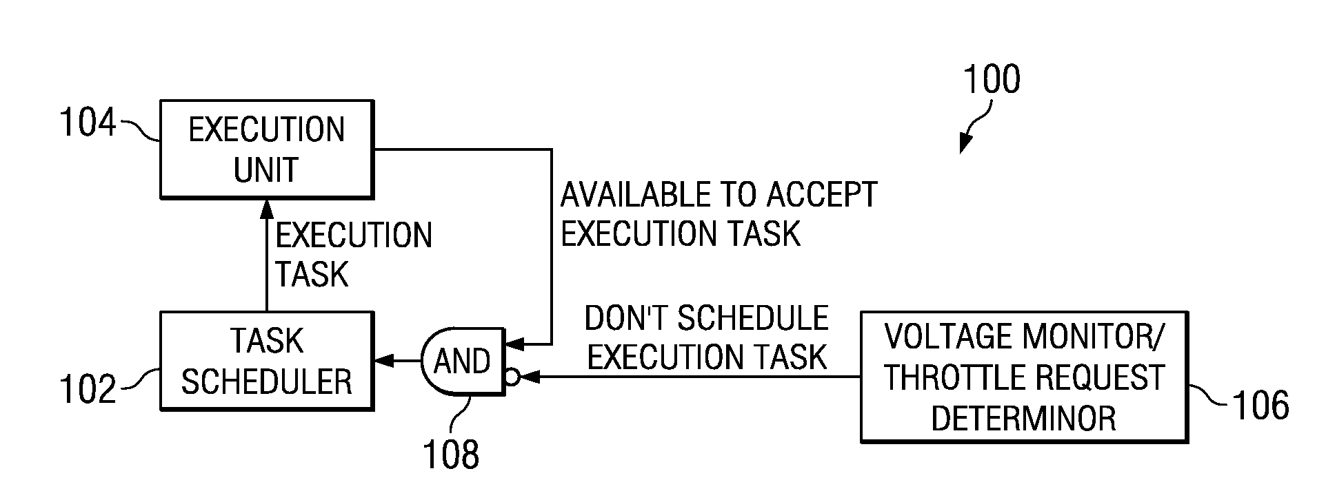
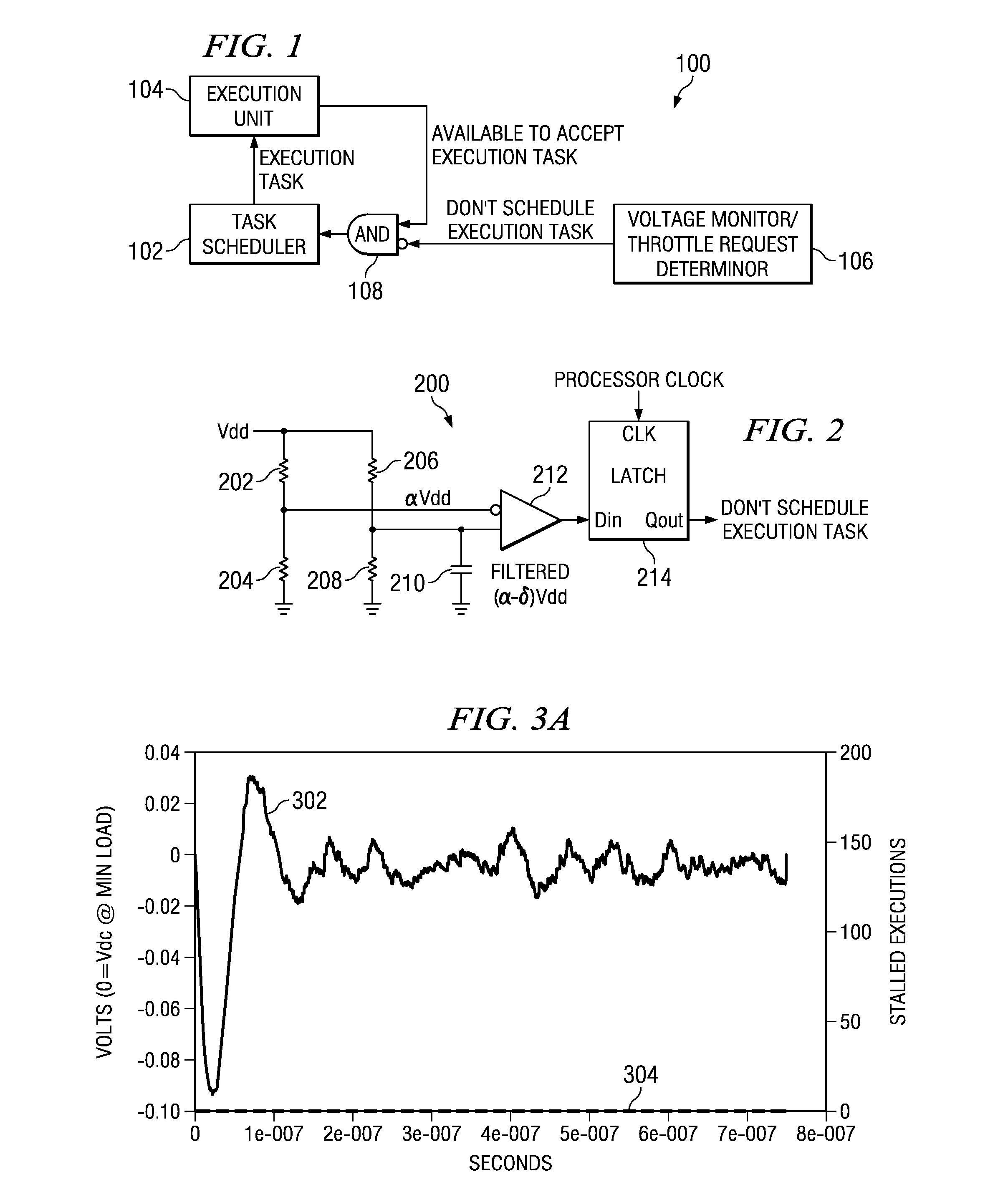
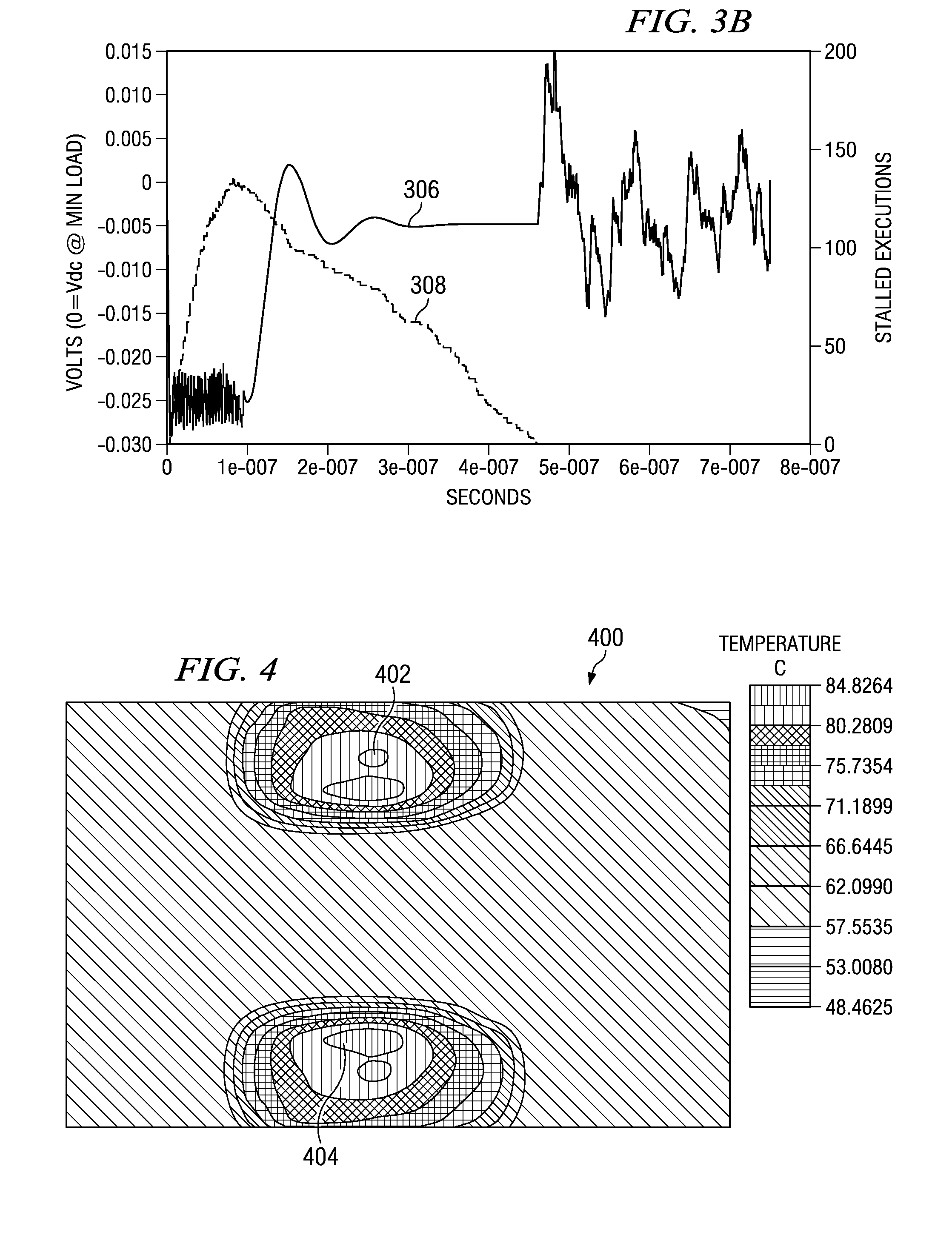
[0033]The illustrative embodiments improve upon the mechanisms referenced in U.S. patent application Ser. No. 11 / 420,825 and U.S. patent application Ser. No. 11 / 420,820, which are herein incorporated in their entirety. The mechanisms in U.S. patent application Ser. Nos. 11 / 420,825 and 11 / 420,820 detect and throttle power-consuming instructions to mitigate on-chip noise and improve chip performance. The illustrative embodiments further optimize frequency, yield, capacitance, and power in a semiconductor chip by customizing or personalizing the location or attribute parameters associated with detecting and throttling power-consuming instructions throughout areas on the chip.

[0034]FIGS. 1-4 are provided first to illustrate the mechanisms for detecting and throttling instruction executions in a microprocessor as described in U.S. patent application Ser. Nos. 11 / 420,825 and 11 / 420,820. A mechanism for throttling executions in a chip is illustrated in FIG. 1, and a mechanism for detecting...


PUM


Abstract

A method and system for applying multiple voltage droop detection and instruction throttling instances with customized thresholds across semiconductor chips. Environmental parameters are detected for various locations on a chip, and timing margins are determined for each location on the chip. An acceptable voltage droop for each location is determined based on the environmental parameters and the timing margins for the corresponding location. A droop threshold is then determined for each location based on the corresponding acceptable voltage droop determined for the corresponding location.

Description

CROSS REFERENCE TO RELATED APPLICATION[0001]The present invention is related to co-pending U.S. patent application Ser. No. ______ (attorney docket no. AUS920070558US1) entitled “Application of Multiple Voltage Droop Detection and Instruction Throttling Instances with Customized Thresholds across a Semiconductor Chip”, filed even date hereof, assigned to the same assignee, and incorporated herein by reference.BACKGROUND OF THE INVENTION[0002]1. Field of the Invention[0003]The present invention relates generally to integrated circuit device design, and in particular to integrated circuit design techniques to mitigate on-chip noise of such device. More particularly, the present invention is directed to applying multiple voltage droop detection and instruction throttling instances with customized thresholds across semiconductor chips.[0004]2. Description of the Related Art[0005]Improvements in manufacturing processes are enabling integrated circuit devices to offer more functionality a...

Claims


Application Information

Patent Timeline
Patent Type & Authority Applications(United States)
IPC IPC(8): G06F19/00
CPCG06F1/28G06F1/305Y02B60/1221G06F1/3237G06F1/3203Y02D10/00
Inventor WEEKLY, ROGER D.
Owner IBM CORP
Why Eureka
Try Eureka