Multiple conductive layer TFT

Active Publication Date: 2009-03-12
FLEXENABLE
View PDF46 Cites 23 Cited by
  • Summary
  • Abstract
  • Description
  • Claims
  • Application Information

AI Technical Summary

Benefits of technology

[0083]The main advantages of the aforementioned 5-layer structure, as described above, are that it reduces the processing and materials constraints on the 4-layer pixel dielectric 7. The sandwich capacitor structure allows a greater capacitance to be achieved, a lower specification of materials to be used and thicker layers, which may be easier to reliably process. The 5-layer structure also encompasses the advantages in terms of alignment tolerant designs and low alignment processing steps that are outlined for the 4-layer structure above.
[0084]The combination of materials and processes used to fabricate this invention are preferably tailored to the end use of the device. For a reflective display, there is no need for the active matrix backplane components to be transparent. However, for a transmissive display, one arrangement uses a combination of high conductivit

Problems solved by technology

Silicon based processes require a combination of vacuum deposition and subtractive photolithographic patterning steps leading to high capital equipment, materials and manufacturing costs.
However, when using printing processes such as inkjet printing, screen printing and offset printing, it is difficult to fabricate metallic interconnect lines with a width of less than 50-100 μm because of the difficulties associated with delivering small volumes of liquid.
However, even using this technique, achieving linewidths of less than 10-20 μm can be challenging.
Furthermore, many printable conductors such as conducting polymers or colloidal metals have conductivities significantly lower than bulk copper or silver, therefore requiring thick and wide interconnect lines to achieve adequate conductance across a large active matrix.
In a conventional pixel architecture for an active matrix application, where the data line, the source and drain electrode of the TFT, the pixel electrode and the pixel capacitor are all defined in the same layer of the device, and compete with each other for space, the limited printing resolution reduces the achievable aperture ratio and front-of-screen performance of the display.
The areas of the gate interconnect lines and the capacitor counter electrode needs to be shielded from the viewer, as the electrical signals on these lines induce undesirable optical contrast of the display element.
In a transmissive display the aperture ratio restrictions are even harder to cou

Method used


Image

  • Multiple conductive layer TFT
  • Multiple conductive layer TFT
  • Multiple conductive layer TFT

Examples


Example

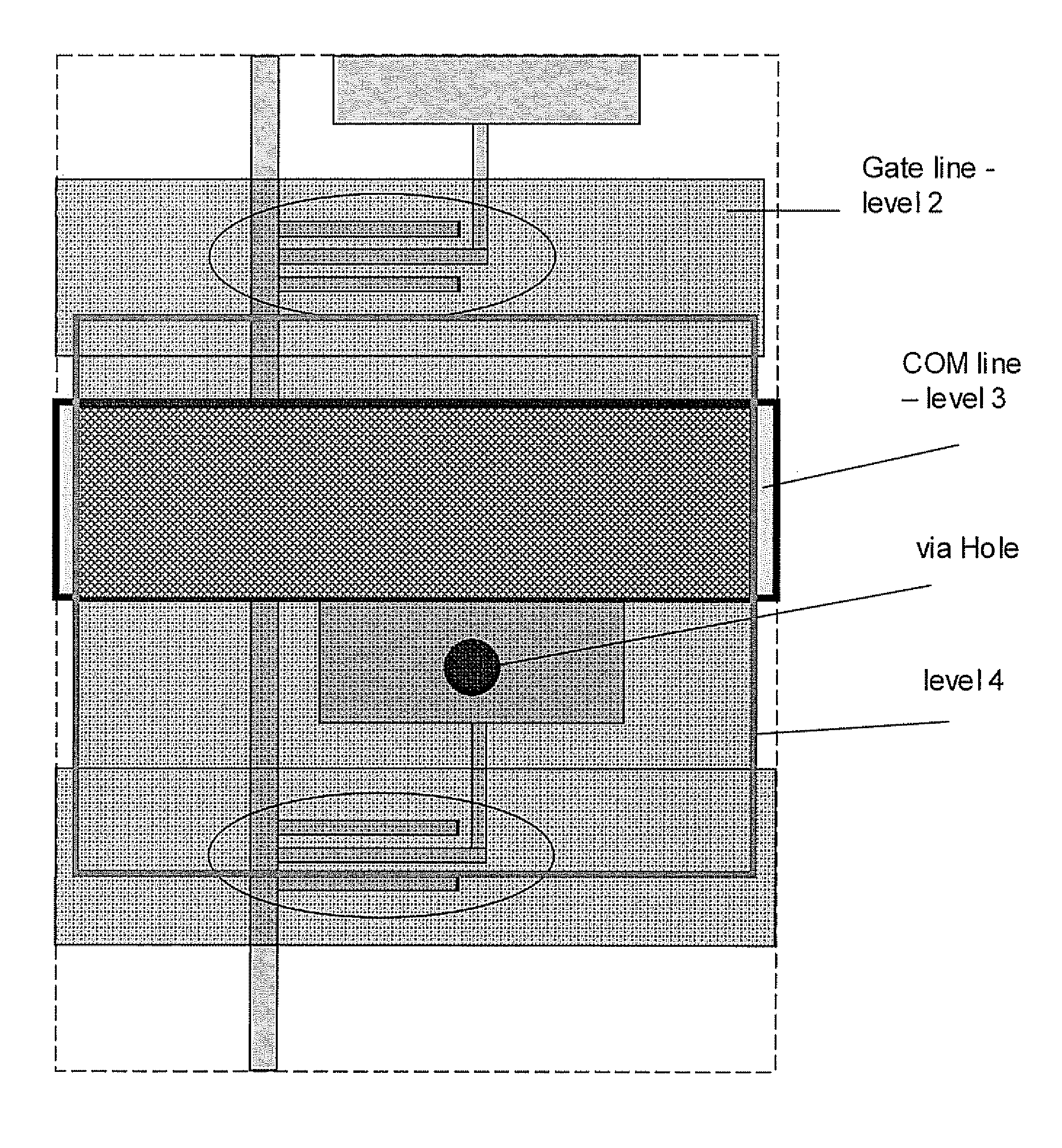
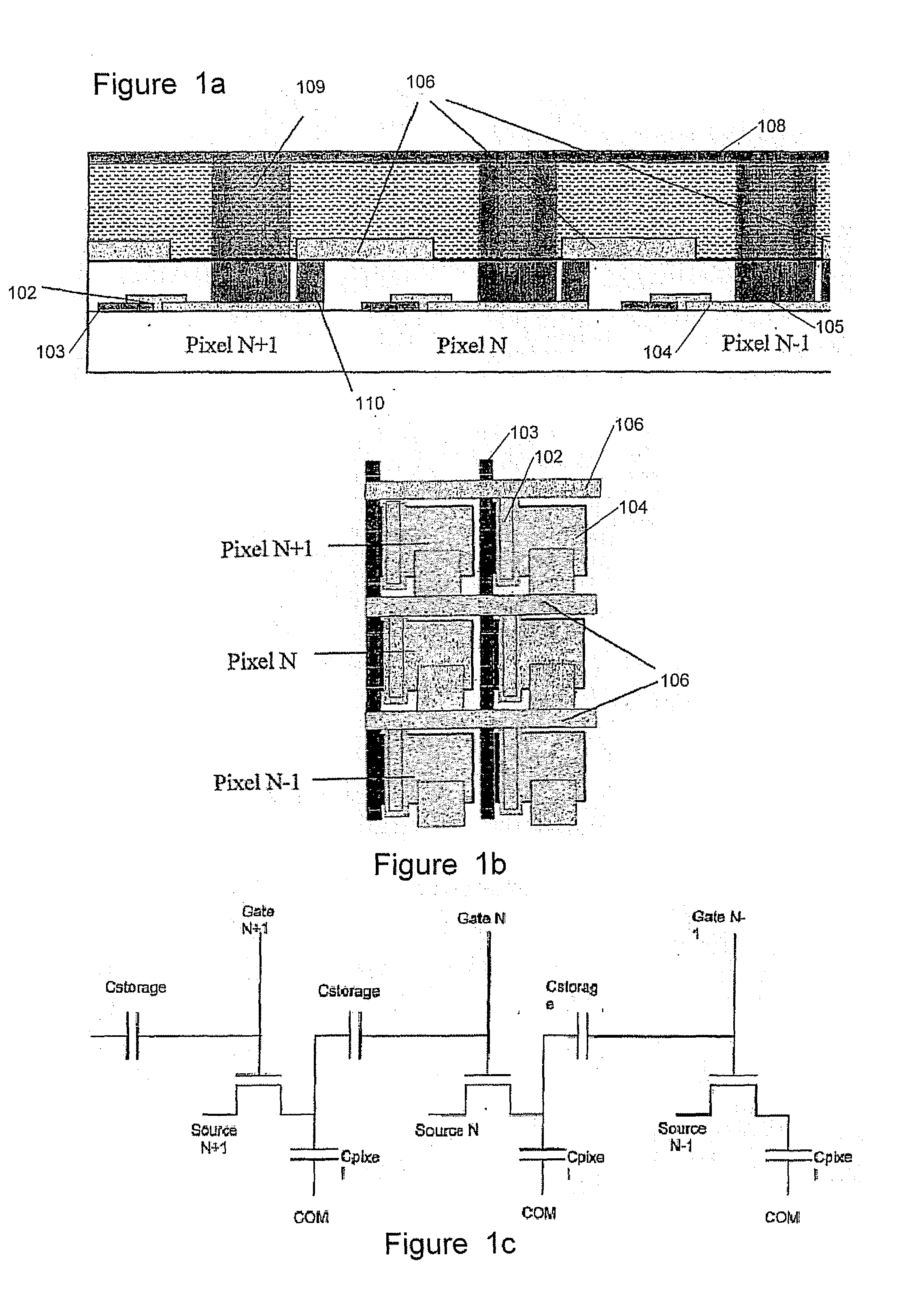
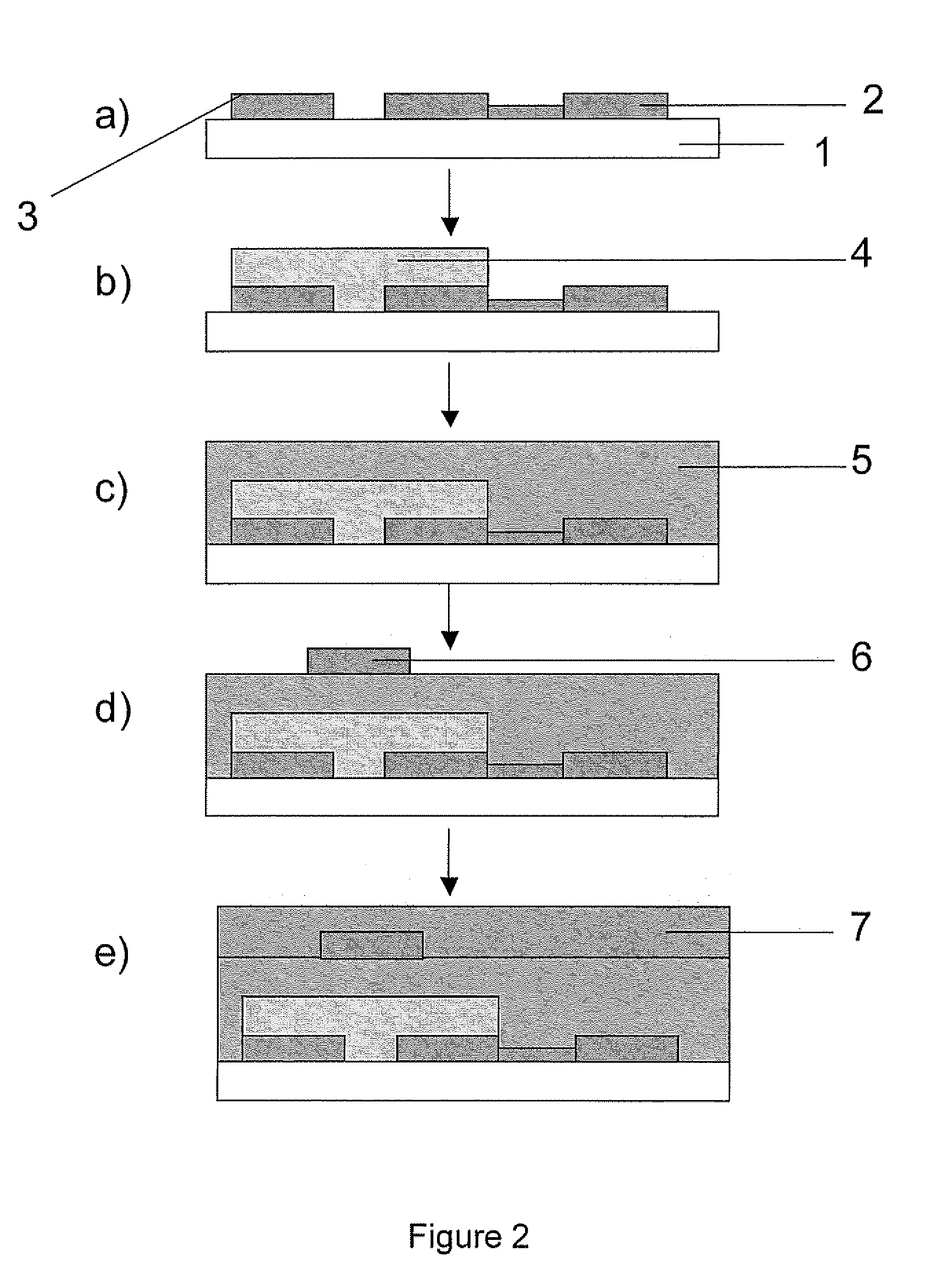
[0060]With reference to FIGS. 2 and 3, a first embodiment of the present invention is now described in detail. A substrate 1 is coated with a thin layer of conductive material. The substrate may be either glass or a polymer film. According to a preferred embodiment of the invention the substrate is a plastic substrate, such as a film of polyethyleneterephtalate (PET) or polyethylenenaphtalene (PEN). A first conductive layer 2, is preferably a metallic layer, and most preferably a layer of inorganic metal such as gold or silver; or any metal that adheres well to the substrate and is electrically compatible with the chosen semi-conductor may also be used, or any combination of metals to achieve these effects. A bilayer structure may be deposited, including a seed or adhesion layer in between the layer of metallic material and the substrate. Alternatively, a conductive polymer may be used, such as PEDOT / PSS. The conductive material is preferably deposited using solution processing tech...

Example

[0074]A second embodiment of the present invention provides a five layer transistor device structure as is illustrated in FIG. 4. As described above, this structure incorporates an additional conductive layer as a capacitor layer and overlying dielectric material layer which allows a lower tolerance for the dielectric layer deposited above the COM layer, for example for thickness of the layer. The addition of both the dielectric layer above the capacitor level and the layer of dielectric material above the COM layer may be used in a capacitor structure where there is a requirement for the capacitance to be high. This five layer sandwich structure is advantageous as it allows a thicker top dielectric layer to be used and allows the patterning of the top pixel electrode to be achieved more readily and allows the possibility of higher Cstorage values.

[0075]With reference to FIG. 4 which continues to FIG. 2, a second embodiment of the present invention is now described. As stated above,...


PUM


Abstract

The present invention relates to a multiple layer pixel architecture for an active matrix display in which a common bus line is formed on a metal level which is separate from that on which the gate electrodes of the TFTs are formed. A multilayer electronic structure adapted to solution deposition, the structure including a thin film transistor (TFT) for driving a pixel of an active matrix optoelectronic device and a capacitor for storing charge to maintain an electrical state of said active matrix pixel, wherein the structure comprises a substrate bearing at least four conducting layers separated by at least three dielectric layers, first and second ones of said conducting layers defining drain/source electrodes and a gate electrode of said transistor respectively, and third and fourth ones of said conducting layers defining respective first and second plates of said capacitor, and wherein said capacitor and said transistor are laterally positioned such that they overlap in a vertical direction.

Description

[0001]The present invention relates to a multiple layer thin film transistor (TFT) structure for use for an active matrix polymer TFT display fabricated using techniques such as solution processing and direct printing.[0002]In accordance with the prior art, multi-layer active matrix displays are well known. Conventional thin film transistors (TFT) are typically fabricated with inorganic silicon, such as amorphous silicon or polycrystalline silicon. Silicon based processes require a combination of vacuum deposition and subtractive photolithographic patterning steps leading to high capital equipment, materials and manufacturing costs. The most common active matrix display technology is the thin film transistor liquid crystal display (LCD, where applications range from PDA and notebook devices to flat screen televisions. Active matrix displays are also used in combination with emerging display effects such as organic light emitting diodes (OLED) and electronic paper (electrophoretic ma...

Claims


Application Information

Patent Timeline
IPC IPC(8): H01L51/00H01L21/00H01L29/786
CPCH01L27/3265H01L27/3262H10K59/1216H10K59/1213H10K19/10H10K10/84H10K10/462H10K59/125H10K59/131H10K71/611H10K59/1201H01L23/5286
Inventor REYNOLDS, KIERANRAMSDALE, CATHERINEJACOBS, KEVINREEVES, WILLIAM
Owner FLEXENABLE
Why Eureka
Try Eureka