Angular velocity detector, method of detection of angular velocities using angular velocity detector, and method of fabricating angular velocity detector
- Summary
- Abstract
- Description
- Claims
- Application Information
AI Technical Summary
Benefits of technology
Problems solved by technology
Method used
Image

Examples
embodiment 1
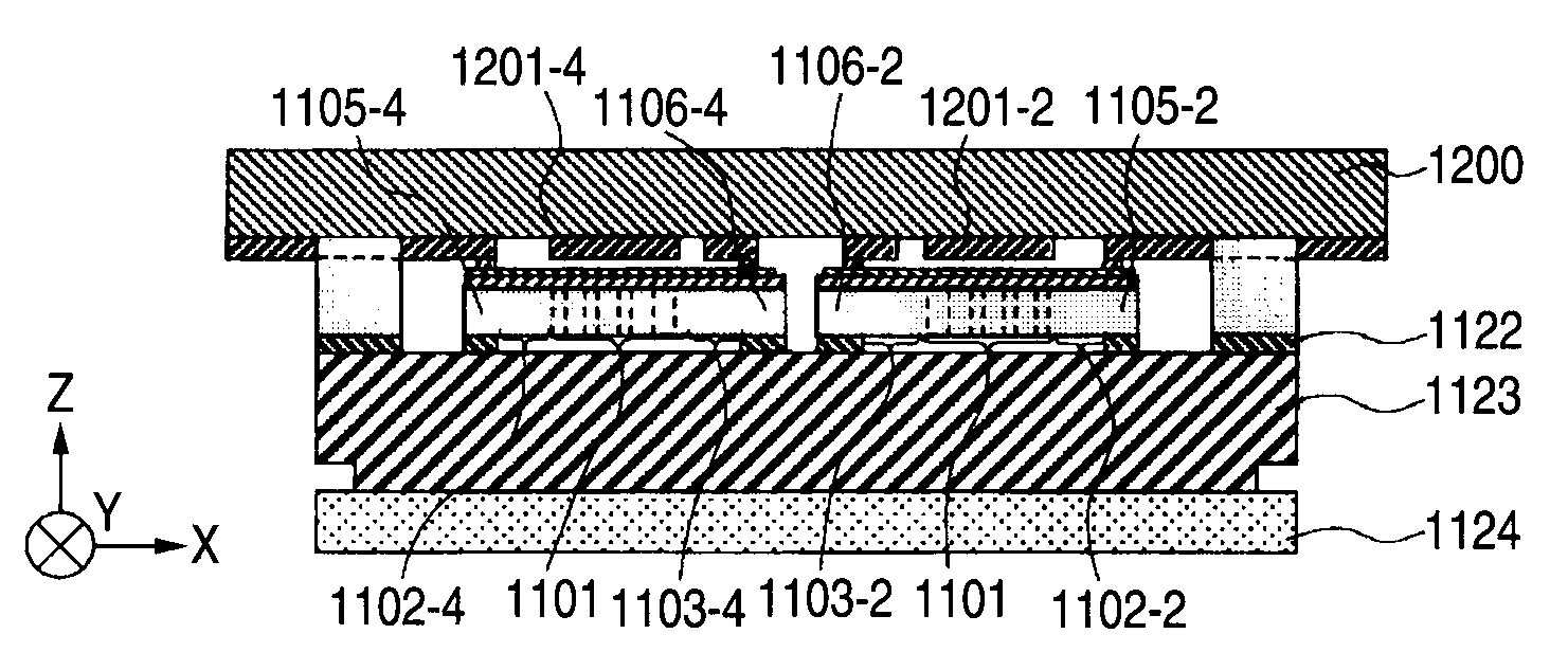
[0100] One embodiment associated with an angular velocity detector of the invention is described by referring to FIGS. 1A and 1B. FIGS. 1A and 1B show the fundamental structure of the angular velocity detector of the invention. FIG. 1A is a schematic plan view of a first substrate as viewed from the electrode shown in FIG. 1B. FIG. 1B is a schematic cross section taken on line A-A′ of FIG. 1A. Note that FIGS. 1A-1B are not always drawn to the same scale.
[0101] As shown in FIGS. 1A-1B, the angular velocity detector of the invention, 1001, is equipped with a vibrator 1101. The vibrator 1101 is made, for example, of an annular thin film. In the figures, four outer springs 1102 (i.e., outer springs 1102-1, 1102-2, 1102-3, and 1102-4) are disposed as a plurality of resilient support bodies outside the vibrator 1101. In the figures, four inner springs 1103 (i.e., inner springs 1103-1, 1103-2, 1103-3, and 1103-4) are disposed as a plurality of resilient support bodies inside the vibrator ...
embodiment 2
[0128] One embodiment associated with a method of fabricating an angular velocity detector of the invention is next described by referring to schematic cross sections and schematic plan views of FIGS. 4A to 13C illustrating a fabrication sequence. Here, as an example, a method of fabricating the angular velocity detector of the above-described Embodiment 1 is described.
[0129] As shown in FIG. 4A, an SOI (silicon-on-insulator) substrate 1150 having the insulator layer 1122 sandwiched between an upper silicon layer 1150-1 and a lower silicon layer 1150-2 is used. The insulator layer 1122 is made, for example, of a film of silicon oxide (SiO2). Here, the lower silicon layer 1150-2 corresponds to the first substrate 1100 of the above-described Embodiment 1. The silicon layer is described as the first substrate 1100. A vibrator and resilient support bodies (such as springs) are fabricated from this SOI substrate 1150. A masking layer 1160 is formed on the surface of the lower silicon la...
embodiment 3
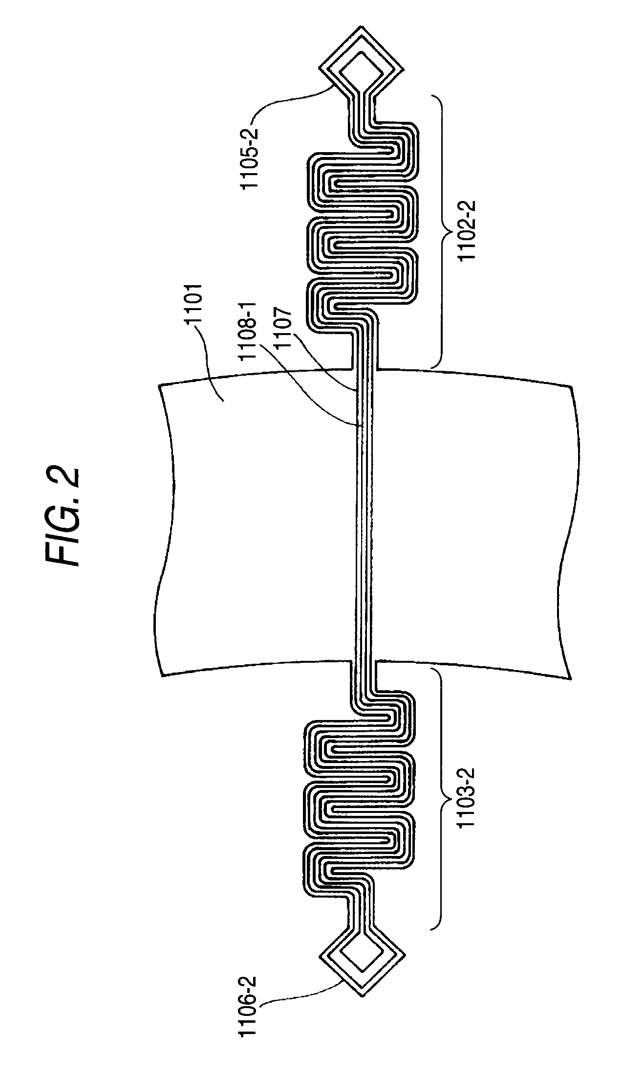
[0147] With respect to the shapes of the inner and outer springs described in the above-described Embodiments 1 and 2, another structure is described next by referring to FIGS. 14-16. As typical ones of them, the outer spring 1102 and inner spring 1103 are shown here. However, the above-described outer spring 1102-1 and inner spring 1103-1, the outer spring 1102-2 and inner spring 1103-2, the outer spring 1102-3 and inner spring 1103-3, and the outer spring 1102-4 and inner spring 1103-4 can also assume a similar structure.
[0148] As shown in FIG. 14, the inner spring 1103 and outer spring 1102 are shaped wavily when viewed on a plane. The number of folds may be one or more. Preferably, the bent portion of each spring is rounded as shown. The rounding improves the durability of the spring. Furthermore, the bent portion of the driver electrode (not shown) formed on each spring is preferably rounded for the same reason as for the springs.
[0149] As shown in FIG. 15, each of the inner ...
PUM
 Abstract
Description
Claims
Application Information