Laser spike annealing for gate dielectric materials

Inactive Publication Date: 2006-11-30
TAIWAN SEMICON MFG CO LTD
View PDF15 Cites 9 Cited by
  • Summary
  • Abstract
  • Description
  • Claims
  • Application Information

AI Technical Summary

Benefits of technology

[0009] In accordance with yet another aspect of the present invention, a capacitor is formed by connecting the source and drain of the MOS device. With laser spike annealed gate dielectric, the capacitor has greater capacitance and is less likely to breakdown.
[0010] An advantageous feature of the present invention is that the gate dielectric layer can be annealed rapidly without causing agglomeration and diffusion.

Problems solved by technology

At such a small dimension, any tunneling through a gate dielectric layer to the underlying channel region significantly increases gate-to-channel leakage current and increases power consumption.
However, high-k materials have a disadvantage that their densities are lower than conventional thermally grown, low-k silicon dioxide.
Conventionally, gate dielectric annealing is performed by rapid thermal annealing (RTA) or furnace annealing, which requires temperature as high as around 700° C. Since wafers are typically kept at high temperature for a long period, conventional rapid thermal annealing and furnace annealing have drawbacks of agglomeration formation, high thermal budget cost, and high diffusion of impurities.
Since gate electrode 6 absorbs laser energy, if not well controlled, the gate electrode may absorb too much energy, causing the gate dielectric to remain below the desired annealing temperature.
The energy absorption is particularly severe when the gate electrode is thick.

Method used


Image

  • Laser spike annealing for gate dielectric materials
  • Laser spike annealing for gate dielectric materials
  • Laser spike annealing for gate dielectric materials

Examples


Embodiment Construction

[0015] The making and using of the presently preferred embodiments are discussed in detail below. It should be appreciated, however, that the present invention provides many applicable inventive concepts that can be embodied in a wide variety of specific contexts. The specific embodiments discussed are merely illustrative of specific ways to make and use the invention, and do not limit the scope of the invention.

[0016] The preferred embodiments are illustrated in FIGS. 2 through 6, wherein like reference numbers are used to designate like elements throughout the various views and illustrative embodiments of the present invention.

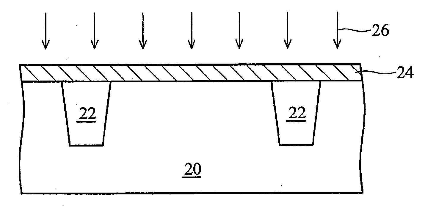
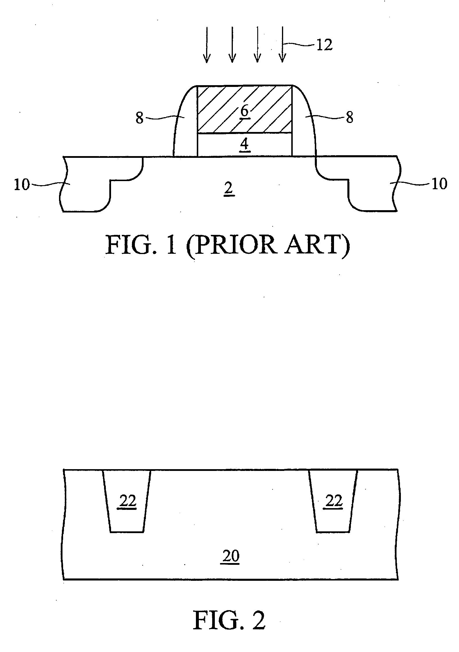
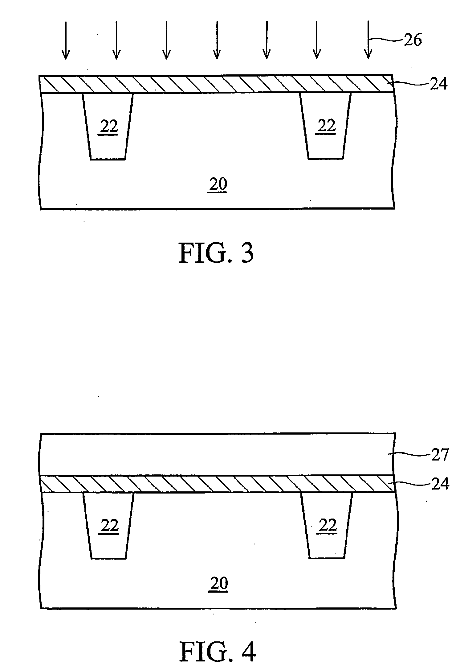
[0017]FIG. 2 illustrates the formation of shallow trench isolations (STI) 22 in a substrate 20. In the preferred embodiment, substrate 20 is a silicon substrate. In other embodiments, substrate 20 comprises other commonly used materials such as germanium, carbon, and / or their combinations. STIs 22 are formed in the substrate 20, preferably by etching shall...


PUM


Abstract

A method of forming a semiconductor device using laser spike annealing is provided. The method includes providing a semiconductor substrate having a surface, forming a gate dielectric layer on the surface of the semiconductor substrate, laser spike annealing the gate dielectric layer, and patterning the gate dielectric layer and thus forming at least a gate dielectric. Source and drain regions are then formed to form a transistor. A capacitor is formed by connecting the source and drain regions.

Description

TECHNICAL FIELD [0001] This invention relates generally to semiconductor devices, specifically to manufacturing processes of semiconductor devices, and more specifically to laser spike annealing of gate dielectrics. BACKGROUND [0002] With semiconductors devices increasingly scaled down, gate dielectrics become thinner with thicknesses approaching about 20 Å or less. At such a small dimension, any tunneling through a gate dielectric layer to the underlying channel region significantly increases gate-to-channel leakage current and increases power consumption. Gate dielectrics are therefore required to have high density and fewer pores. [0003] High-k materials are commonly used as gate dielectrics for MOSFET devices. However, high-k materials have a disadvantage that their densities are lower than conventional thermally grown, low-k silicon dioxide. One of the methods of improving density is annealing, by which the material density is increased and thus electrical properties are improv...

Claims


Application Information

Patent Timeline
IPC IPC(8): H01L21/336
CPCH01L21/268H01L21/28185H01L29/6659H01L29/517H01L29/665H01L29/513
Inventor YAO, LIANG-GIYANG, MING-HOCHEN, SHIH-CHANGLIANG, MONG SONG
Owner TAIWAN SEMICON MFG CO LTD
Why Eureka
Try Eureka