Pixel structure and forming method and driving method thereof

a technology of liquid crystal display and pixel structure, which is applied in the direction of optics, instruments, electrical appliances, etc., can solve the problems of delay of the entire display panel, lc response is slower than mva mode, and light leakage during the dark state at this region

Active Publication Date: 2009-03-12
AU OPTRONICS CORP
View PDF4 Cites 5 Cited by
  • Summary
  • Abstract
  • Description
  • Claims
  • Application Information

AI Technical Summary

Benefits of technology

[0010]According to an embodiment of the present invention, a pixel structure, disposed on a first substrate and electrically coupled to at least one scan line and at least one data line, the pixel structure comprises: a first switch device electrically coupled to the scan line and the data line; a second switch device electrically coupled to the scan line and the data line; at least one pixel electrode electrically coupled to the second switch device; at least one control electrode electrically coupled to the first switch element; and at least one coupling electrode disposed under a portion of the control electrode.
[0011]According to another embodiment of the present invention, a method for forming a pixel structure, the pixel structure disposed on a first substrate and electrically coupled to at least one scan line and at least one data line, the method comprises: forming a first switch device in the pixel structure electrically coupling to the scan line and the data line; forming a second switch device in the pixel structure electrically coupling to the scan line and the data line; forming at least one pixel electrode in the pixel structure electrically coupling to the second switch device; forming at least one control electrode in the pixel structure electrically coupling to the first switch element; and forming at least one coupling electrode disposed under a portion of the control electrode.
[0012]According to still another embodiment of the present invention, a method for driving a pixel structure, the pixel structure disposed on a first substrate and electrically coupled to at least one scan line and at least one data line, and the pixel structure having a first switch device, a second switch device, at least one pixel electrode, at least one control electrode, and at least one coupling electrode, the method comprises: providing a voltage corresponding to a displaying data to the pixel electrode and the control electrode, such that the pixel and the control electrode are at a floating connection state; providing a first coupling voltage to the coupling electrode; and coupling a variation of the first coupling voltage to the control electrode via at least one coupling capacitor, such that an absolute value of a voltage difference between the control electrode and a common electrode substantially greater than an absolute value of a voltage difference between the pixel electrode and the common electrode, wherein the common electrode is disposed on a second substrate and the second substrate is corresponding to the first substrate.
[0013]The present invention provides a pixel structure configured with a driving design to stably drive voltage on the control electrode such that an absolute value of voltage difference between the control electrode and the common electrode of the upper substrate substantially greater than an absolute value of voltage difference between the pixel electrode and the common electrode of the upper substrate.

Problems solved by technology

Second, since protrusions on the upper substrate of the MVA mode result in a pre-tilt angle of the LC molecules, light leakage during the dark state can occur at this region.
Third, since the PVA mode does not have a pre-tilt angle, LC response is slower than the MVA mode.
If not done the above-mentioned processes and / or alignment requested, the response at the left and right regions of a pixel can be inconsistent, further resulting in response delay of the entire display panel and simultaneously creating an additional disclination line, thus reducing transparency.
The drawbacks of this driving method are: first, an additional set of driving integrated circuit is needed resulting in higher production costs; and second, the driving integrated circuit of the conventional LCD panel does not support this driving method.
However, this driving method has the following problems.
First, the pixel electrode is under a floating state, so static charges are prone to accumulate on the electrode without drainage paths, thereby resulting in image sticking.
Second, since the pixel electrode voltage is generated by coupling capacitance Cc, the voltage on the pixel electrode is lower the conventional driving voltage of the pixel electrode, resulting in deteriorated transparency.
This kind of driving integrated circuit is difficult to fabricate and has higher power consumption.
Second, there are too many thin film transistors in a single pixel, thereby increasing production complexity.

Method used


Image

  • Pixel structure and forming method and driving method thereof
  • Pixel structure and forming method and driving method thereof
  • Pixel structure and forming method and driving method thereof

Examples


Embodiment Construction

[0039]It is to be understood that the following disclosure provides many different embodiments, or examples, for implementing different features of various embodiments. Specific examples of components and arrangements are described below to simplify the present disclosure. These are merely examples and are not intended to be limiting. In addition, the present disclosure may repeat reference numerals and / or letters in the various examples. This repetition is for the purpose of simplicity and clarity and does not in itself indicate a relationship between the various embodiments and / or configurations discussed. Moreover, the formation of a first feature over or on a second feature in the description that follows may include embodiments in which the first and second features are formed in direct contact or not in direct contact.

[0040]FIG. 7 is a circuit diagram for driving a pixel according to an embodiment of the present invention. The circuit diagram for driving a pixel includes a fir...


PUM

PropertyMeasurementUnit
response timeaaaaaaaaaa
driving voltageaaaaaaaaaa
transmission voltageaaaaaaaaaa

Abstract

A pixel structure, disposed on a first substrate, and electrically coupled to at least one scan line and at least one data line is provided. The pixel structure includes a first switch device, a second switch device, at least one pixel electrode, at least one control electrode, and at least one coupling electrode. The first switch device is electrically coupled to the scan line and the data line. The second switch device is electrically coupled to the scan line and the data line. The pixel electrode is electrically coupled to the second switch device. The control electrode is electrically coupled to the first switch element. The coupling electrode is disposed under the control electrode.

Description

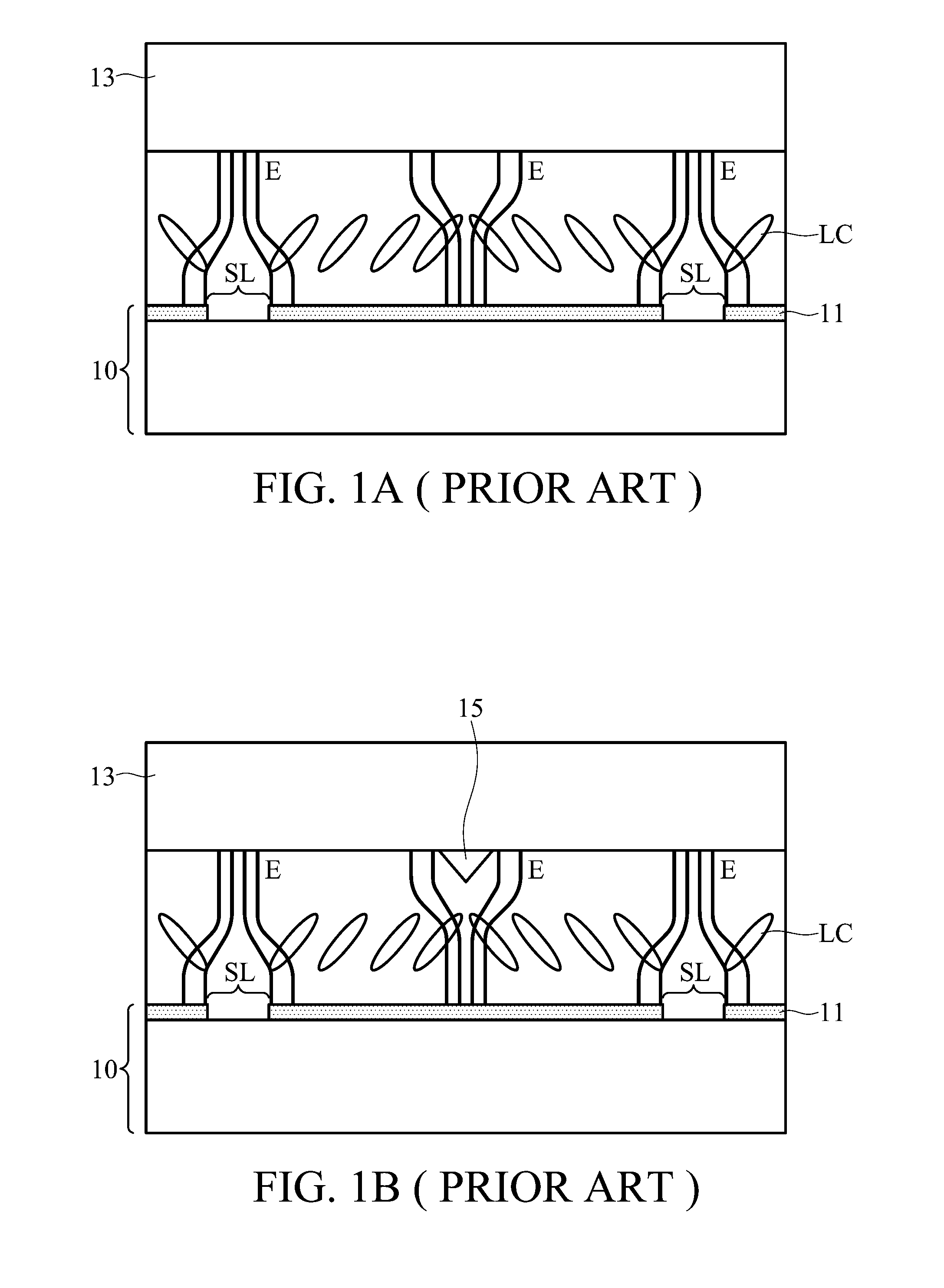
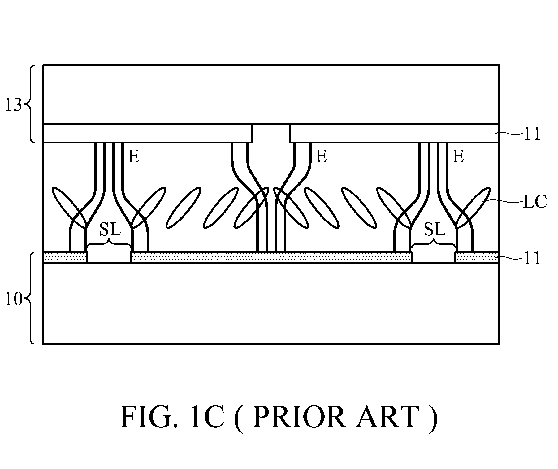
CROSS REFERENCE TO RELATED APPLICATIONS [0001]This application claims the benefit of Taiwan Application No. 096133206, filed on Sep. 6, 2007, the contents of which are incorporated by reference in its entirety.BACKGROUND OF THE INVENTION [0002]1. Field of the Invention[0003]The present invention relates to pixel structures and, more particularly, to pixel structures of liquid crystal display (LCD) devices.[0004]2. Description of the Related Art[0005]FIG. 1A, FIG. 1B, and FIG. 1C are cross sections of pixel structures of a vertical alignment (VA) mode, a multi-domain vertical alignment (MVA) mode, and patterned vertical alignment (PVA) mode, respectively. Generally, concerning the vertical alignment (VA) mode, a lower substrate 10 includes a transparent electrode 11 (e.g., indium tin oxide (ITO)) with a slits SL design such that rotation of the liquid crystal (LC) molecules is consistent with distribution of the electric field E generated therefrom. Regarding the multi-domain vertica...

Claims


Application Information

Patent Timeline
Patent Type & Authority Applications(United States)
IPC IPC(8): G09G3/36G02F1/136H01L21/84
CPCG02F2001/134345G02F2001/134354G09G3/3648G09G2310/06G09G2300/0447G09G2300/0814G09G2300/043G02F1/134345G02F1/134354
Inventor SU, JENN-JIATIEN, MING-FENGYANG, CHIA-JUNGCHANG, TING-JUICHEN, PO-LUN
Owner AU OPTRONICS CORP
Why Eureka
Try Eureka