Pixel structure and liquid crystal display panel

Active Publication Date: 2009-03-12
AU OPTRONICS CORP
View PDF12 Cites 11 Cited by
  • Summary
  • Abstract
  • Description
  • Claims
  • Application Information

AI Technical Summary

Benefits of technology

[0025]Based on the above described, the present invention makes a single second conductive region of the semiconductor layer electrically connected to the data line and uses different channel regions to input a same signal delivered by the data line to the first transparent electrode and the second transparent electrode respectively, so that the different transparent electrodes in each pixel produce different electrical fields to improve color shift phenomena. Meanwhile, in

Problems solved by technology

In other words, when an angle (φ, θ) of viewing is changed, the frame luminance of a conventional NVA LCD varies, which further leads to color shift or color washout problem.
Although the above-mentioned technique is able to improve color shift, but an additional transistor is usually employed so as to stabilize the data voltage produced by the above-mentioned capacitor coupling effect, but the added transistors would decrease the aperture ratio o

Method used


Image

  • Pixel structure and liquid crystal display panel
  • Pixel structure and liquid crystal display panel
  • Pixel structure and liquid crystal display panel

Examples


Embodiment Construction

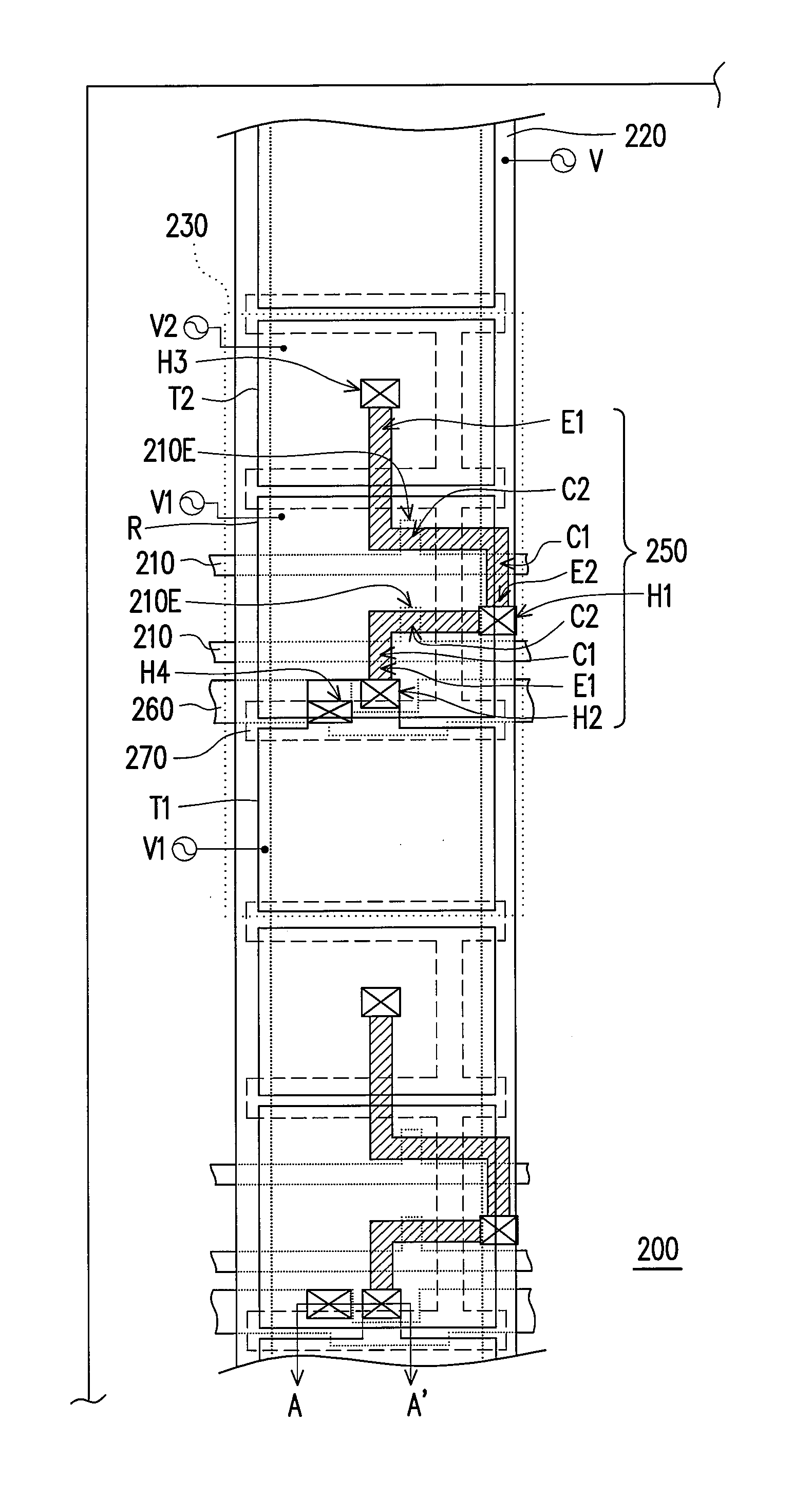
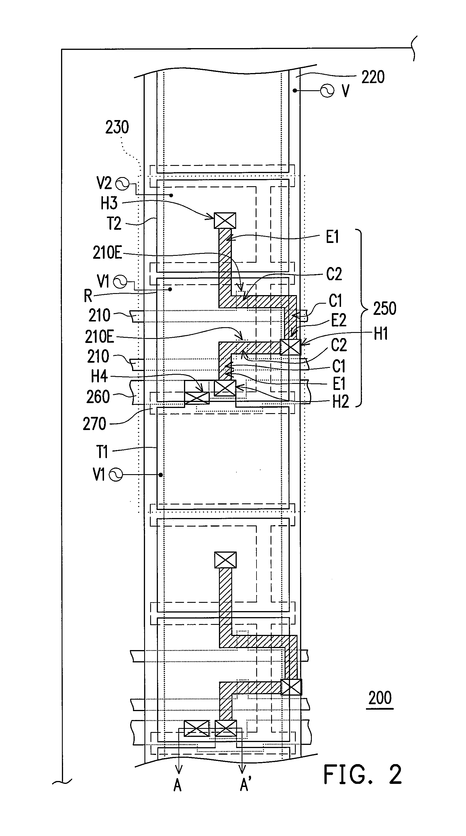
[0038]Reference will now be made in detail to the present preferred embodiments of the invention, examples of which are illustrated in the accompanying drawings. Wherever possible, the same reference numbers are used in the drawings and the description to refer to the same or like parts.

[0039]FIG. 2 is a diagram of an active device array substrate according to the present invention. Referring to FIG. 2, an active device array substrate 200 includes a plurality of scan lines 210, a plurality of data lines 220 and a plurality of pixels 230. In FIG. 2, only some pixels 230 of the active device array substrate 200 are shown. Each of the pixels 230 is electrically connected to two of the scan lines 210 and one of the data line 220 correspondingly, and each of the pixels 230 includes a reflective electrode R, a first transparent electrode T1, a second transparent electrode T2 and a semiconductor layer 250. The first transparent electrode T1 is electrically connected to the reflective elec...


PUM


Abstract

A pixel structure disposed on a substrate and electrically connected to two scan lines and a data line is provided. The pixel structure includes a reflective electrode, a first transparent electrode, a second transparent electrode and a semiconductor layer. The first transparent electrode is electrically connected to the reflective electrode and is insulated from the second transparent electrode. The semiconductor layer has two first conductive regions, a second conductive region and two first channel regions, wherein the first conductive regions are respectively electrically connected to the reflective electrode and the second transparent electrode, the second conductive region is located between the first conductive regions and electrically connected to the data line, a part of the semiconductor layer overlapped with the scan lines is defined as first channel regions and each of the first channel regions is respectively electrically connected between the second conductive region and each first conductive region.

Description

CROSS-REFERENCE TO RELATED APPLICATION[0001]This application claims the priority benefit of Taiwan application serial no. 96133819, filed on Sep. 11, 2007. The entirety of the above-mentioned patent application is hereby incorporated by reference herein and made a part of this specification.BACKGROUND OF THE INVENTION[0002]1. Field of the Invention[0003]The present invention relates to a liquid crystal display panel (LCD panel), and more particularly, to an active device array substrate.[0004]2. Description of Related Art[0005]The market today requires a thin film transistor liquid crystal display (TFT-LCD) to have high contrast ratio, no gray scale inversion, less color shift, high luminance, high chroma, high color saturation, fast response and wide viewing angle. It is available for a TFT-LCD to provide a wide viewing angle nowadays that a technology of twisted nematic liquid crystal (TN liquid crystal) plus wide viewing film, in-plane switching LCD (IPS LCD), fringe field switch...

Claims


Application Information

Patent Timeline
IPC IPC(8): G02F1/1335G02F1/1343
CPCG02F2001/134345G02F1/13624G02F1/134345
Inventor TSAI, MENG-CHANGCHENG, TSUNG-CHINHU, CHIH-JEN
Owner AU OPTRONICS CORP
Why Eureka
Try Eureka