Electronic device mounting structure
a technology for mounting structures and electronic devices, applied in the direction of electrical apparatus casings/cabinets/drawers, lighting and heating apparatus, instruments, etc., can solve the problems of difficult to put the structure disclosed in u.s. pat. no. 7 and the temperature of the electronic device becomes high, so as to improve the cooling performance and manufacturability
- Summary
- Abstract
- Description
- Claims
- Application Information
AI Technical Summary
Benefits of technology
Problems solved by technology
Method used
Image

Examples
first embodiment
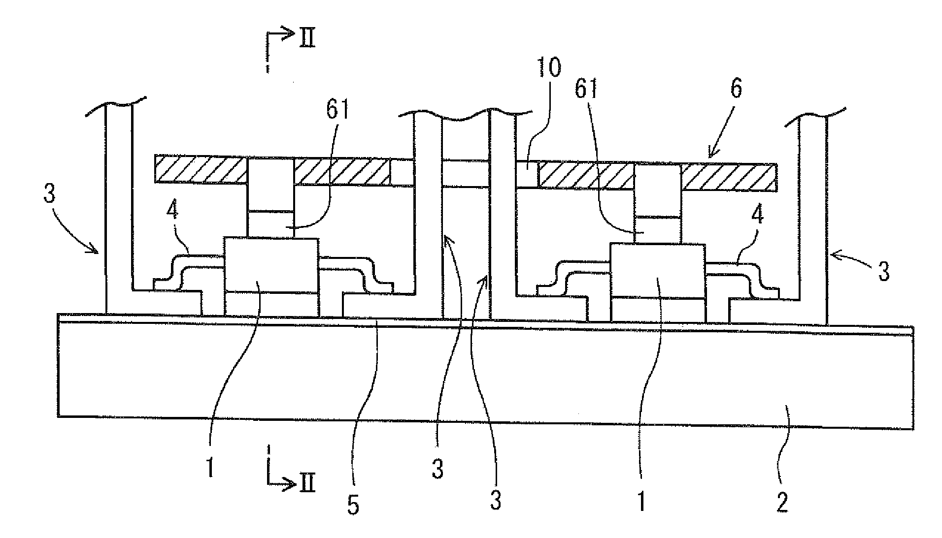
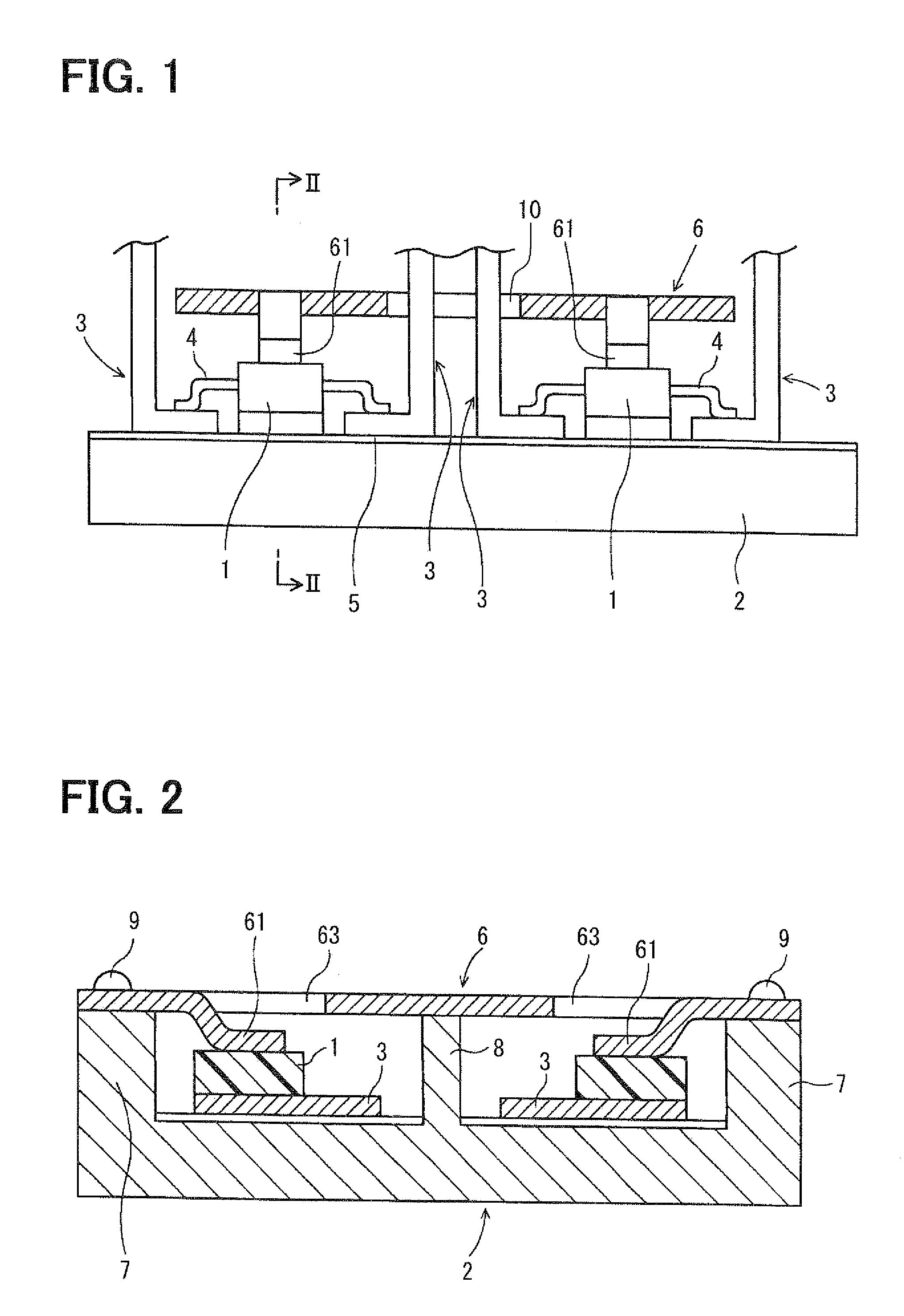
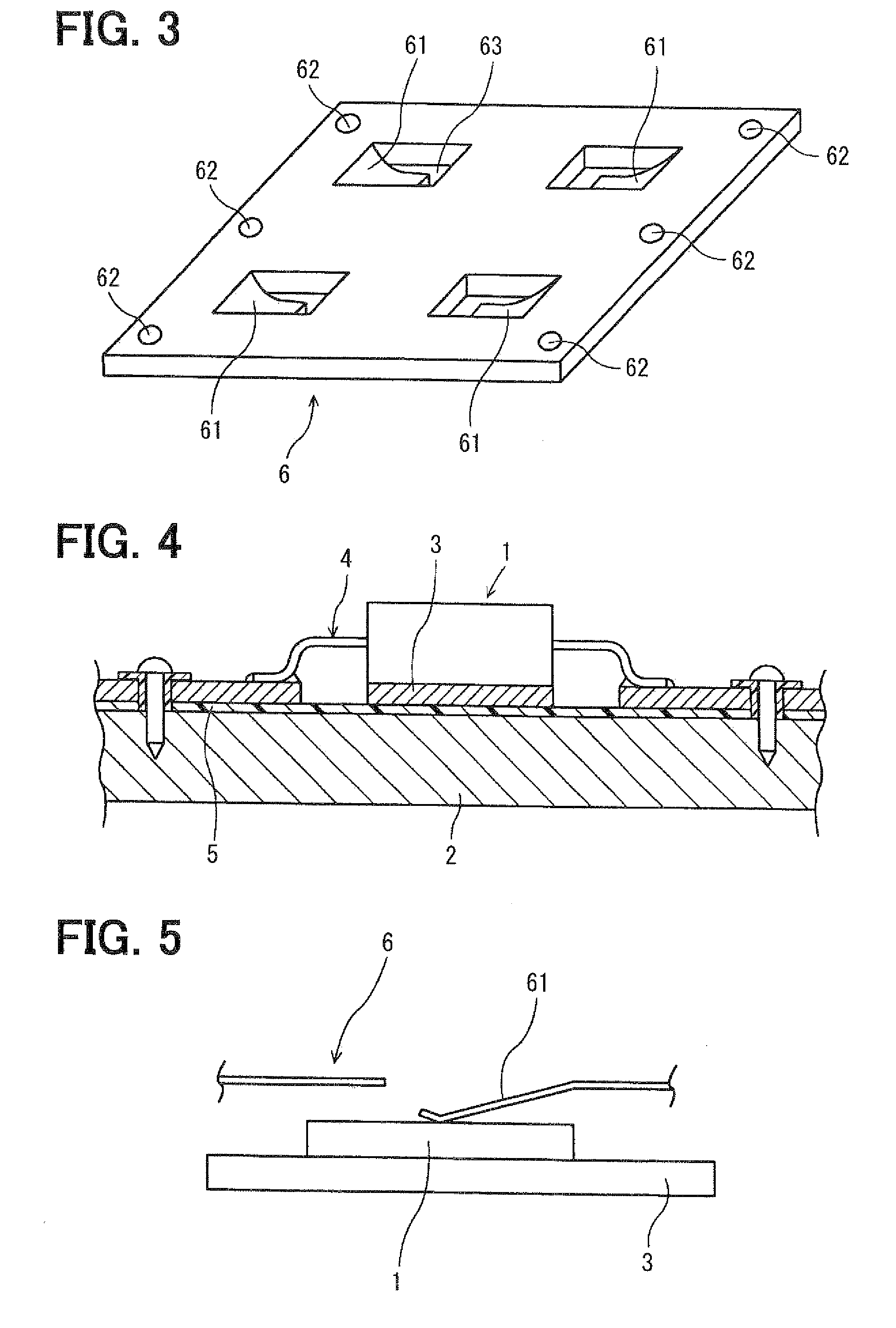
[0021]An electronic device mounting structure according to a first embodiment of the present invention is described below with reference to FIGS. 1-4. The mounting structure includes electronic devices 1, a base plate 2, busbars 3, an electrical insulation film 5 such as a resin film, and an elastic biasing member 6, a pair of wall members 7, and a column member 8.
[0022]Each electronic device 1 has a resin body and lead terminals 4 protruding from each side of the body. That is, the electronic device 1 is a resin-molded integrated circuit (IC) configured as a dual in-line package (DIP). Alternatively, the electronic device 1 can be a ceramic-packaged IC and configured as a single in-line package (SIP), or the like.
[0023]The wall members 7 are integrally formed with the base plate 2, for example, by aluminum die casting. Likewise, the column member 8 is integrally formed with the base plate 2, for example, by aluminum die casting. The busbars 3 and the lead terminal 4 are made of cop...
second embodiment
[0043]An electronic device mounting structure according to a second embodiment of the present invention is described below with reference to FIGS. 7 and 8. A difference between the first and second embodiments is as follows. In the second embodiment, two pressing members 61 facing with each other are paired. The pair of pressing members 61 is configured to press the top surface of the body of the corresponding electronic device 1 against the base plate 2 through the busbar 3. In such an approach, the electronic device 1 can be tightly pressed against the base plate 2. Further, the pressing force can be substantially uniform over the electronic device 1.
third embodiment
[0044]An electronic device mounting structure according to a third embodiment of the present invention is described below with reference to FIGS. 9 and 10. A difference between the first and third embodiments is as follows.
[0045]In the third embodiment, as shown in FIG. 10, two separate elastic biasing members 6A, 6B are used instead of the single elastic biasing member 6. Each of the elastic biasing members 6A, 6B is shaped like a long narrow plate and has two pressing members 64. The elastic biasing members 6A, 6B are arranged parallel to each other so that a predetermined space can be maintained between the elastic biasing members 6A, 6B. The space can be used as the slit 10, through which the busbar 3 passes.
[0046]The elastic biasing members 6A, 6B are the same in structure. FIG. 9 illustrates the elastic biasing member 6A. As shown in FIG. 9, each pressing member 64 is shaped like a rectangular recess. Specifically, the pressing member 64 has a flat portion 64A and leg portions...
PUM
 Abstract
Description
Claims
Application Information
 - Generate Ideas
- Intellectual Property
- Life Sciences
- Materials
- Tech Scout
- Unparalleled Data Quality
- Higher Quality Content
- 60% Fewer Hallucinations
Browse by: Latest US Patents, China's latest patents, Technical Efficacy Thesaurus, Application Domain, Technology Topic, Popular Technical Reports.
© 2025 PatSnap. All rights reserved.Legal|Privacy policy|Modern Slavery Act Transparency Statement|Sitemap|About US| Contact US: help@patsnap.com