Semiconductor Package Having Socket Function, Semiconductor Module, Electronic Circuit Module and Circuit Board with Socket

a technology of semiconductor modules and socket functions, applied in the direction of electrical apparatus contruction details, printed circuit non-printed electric components association, coupling device connections, etc., can solve the problem of adversely affecting a part which has been already bonded by heat, and achieve the effect of convenient measuremen

Inactive Publication Date: 2009-03-12
APOLLOWAVE CORP
View PDF14 Cites 29 Cited by
  • Summary
  • Abstract
  • Description
  • Claims
  • Application Information

AI Technical Summary

Benefits of technology

[0034]In accordance with the circuit board with the socket, because the circuit board with the socket comprises the socket board mounted on the circuit board, the socket board comprising the socket formed on the top surface of the socket board for enabling electrical conductivity and the connecting terminal formed on the bottom surface of the socket board for enabling electrical conductivity, wherein the socket has the depressed shape, the spiral contact is formed in the depression, and the connecting terminal is bonded to the circuit board and electrically connected to the circuit board, a test board and the like can be readily measured and the semiconductor module and the circuit board can be electrically bonded securely without soldering and heating, whereby the electronic circuit module can be constructed.

Problems solved by technology

However, when the semiconductor devices are stacked and electrically bonded to each other, it has been necessary to heat the semiconductor devices to melt solder.
There has been a problem that the heating adversely affects a part which has been already bonded.
Generally, a semiconductor package incorporates a semiconductor chip; however, the semiconductor package may not incorporate the semiconductor chip.

Method used


Image

  • Semiconductor Package Having Socket Function, Semiconductor Module, Electronic Circuit Module and Circuit Board with Socket
  • Semiconductor Package Having Socket Function, Semiconductor Module, Electronic Circuit Module and Circuit Board with Socket
  • Semiconductor Package Having Socket Function, Semiconductor Module, Electronic Circuit Module and Circuit Board with Socket

Examples


Embodiment Construction

[0058]A semiconductor package having a socket function, a semiconductor module, an electronic circuit module, and a circuit board with a socket according to the present invention are described with reference to the accompanying drawings.

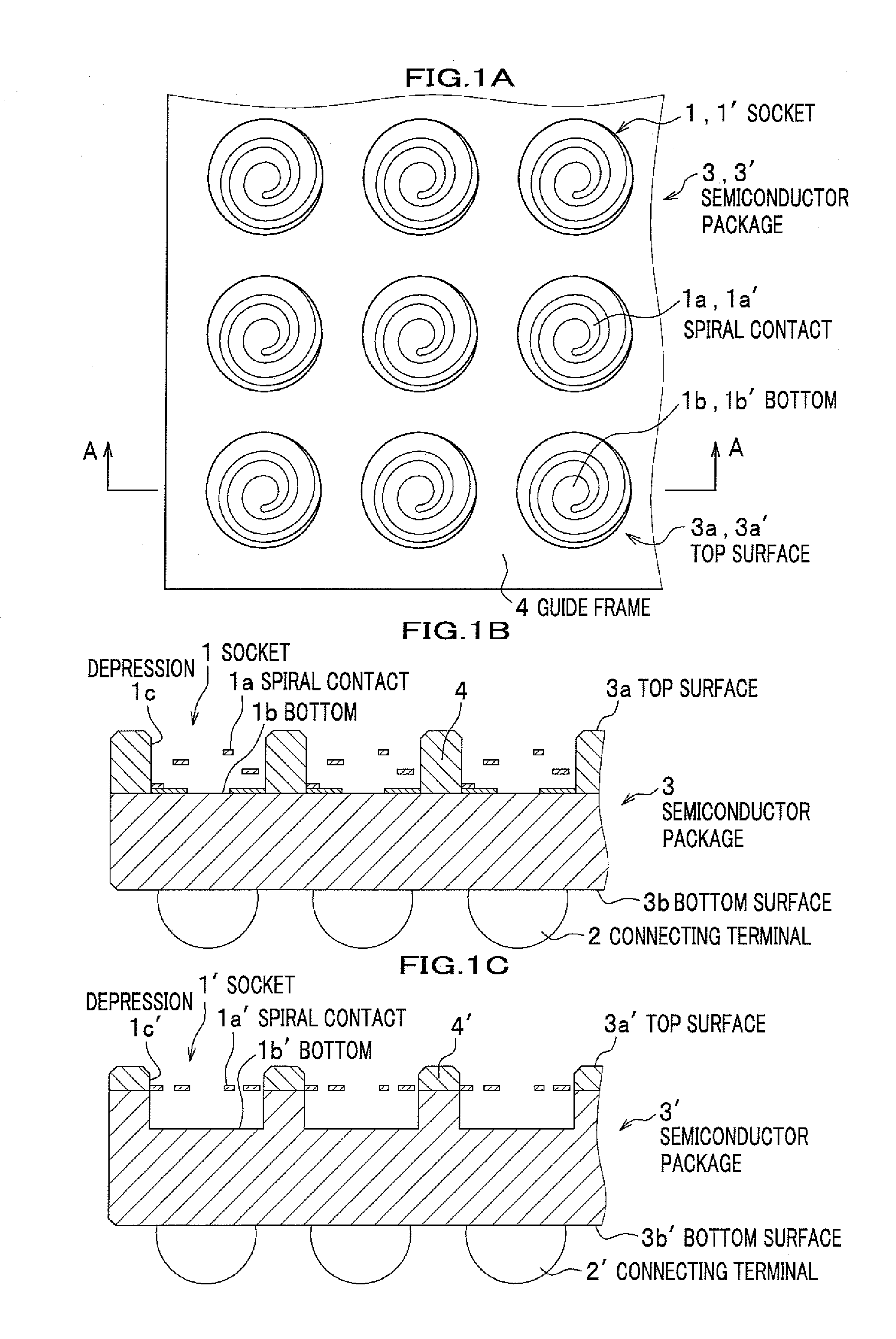
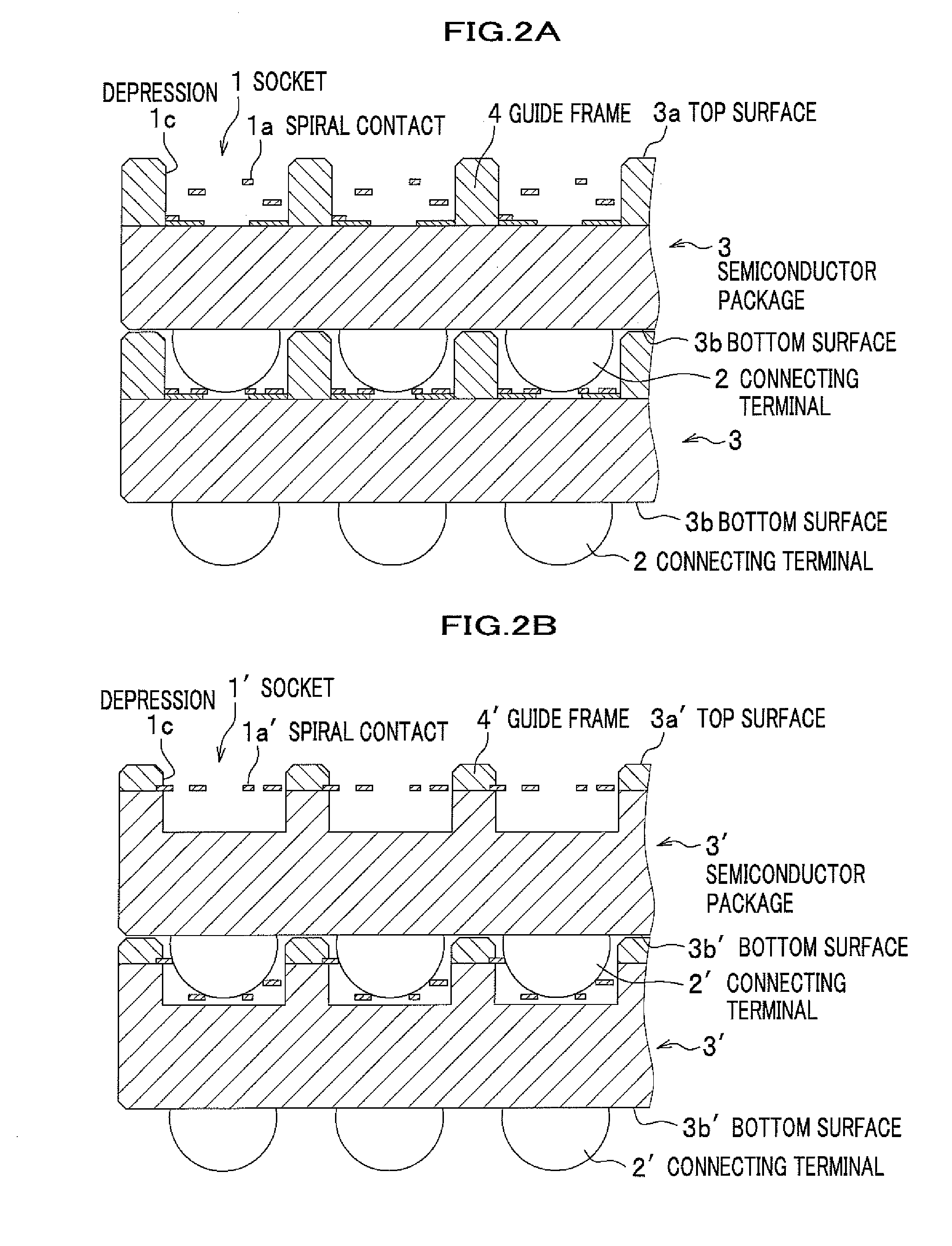
[0059]FIG. 1A is a plain view of a semiconductor package according to an embodiment. FIG. 1B is a cross sectional view of the semiconductor package along A-A line in FIG. 1A, showing conic spiral contacts. FIG. 1C is a cross sectional view of the semiconductor package along A-A line in FIG. 1A, showing horizontal spiral contacts.

[0060]As shown in FIG. 1A, a plurality of sockets 1, 1′ including spiral contacts 1a, 1a′ is formed on the top surface 3a, 3a′ of a semiconductor package 3, 3′.

[0061]As shown in FIG. 1B, the semiconductor package 3 includes the socket 1 formed on the top surface 3a for enabling electrical conductivity and a connecting terminal 2 formed on the bottom surface 3b for enabling electrical conductivity. The connecting terminal 2 is...


PUM


Abstract

Disclosed is a semiconductor package 3 including a socket 1 which is formed on the top surface 3a for enabling electrical conductivity and a connecting terminal 2 which is formed on the bottom surface 3b for enabling electrical conductivity. The socket 1a has a depressed shape, and a spiral contact 1 is formed in the depression 1c. An electronic circuit module is constructed by mounting and electrically connecting a semiconductor module wherein a plurality of semiconductor packages 3 is stacked on a circuit board. A circuit board with sockets is constructed by mounting a socket board on a circuit board.

Description

FIELD OF THE INVENTION[0001]The present invention relates to a semiconductor package having a socket function, a semiconductor module wherein the semiconductor packages are stacked one above the other and / or disposed side by side, an electronic circuit module constructed by mounting the semiconductor module on a circuit board, and a circuit board with a socket.BACKGROUND ART[0002]A stack semiconductor device wherein a plurality of semiconductor devices is stacked and bonded by connecting terminals which are provided on the bottoms of thin semiconductor device packages and formed of solder balls has been conventionally known as an example of stack semiconductor devices. Such a stack semiconductor device is described below with reference to U.S. Pat. No. 6,303,997 (refer to pages 5, 6 and FIG. 3). FIG. 17 is a structural drawing of such a stack semiconductor device. A Semiconductor chip 51 is bonded to an inner lead 53 by adhesive agent 52. The inner lead 53 is electrically connected ...

Claims


Application Information

Patent Timeline
Patent Type & Authority Applications(United States)
IPC IPC(8): H01L23/48H01L23/00H05K7/20H01R12/14H01L23/12H01L25/10H01L25/11H01L25/18H01R13/24H01R33/76H05K1/02H05K1/14H05K1/18
CPCH01L23/3107H01L2225/1082H01L23/467H01L23/473H01L23/4951H01L23/49811H01L24/72H01L25/105H01L2224/16H01L2224/48091H01L2224/4824H01L2224/73215H01L2924/01029H01L2924/01033H01L2924/01078H01L2924/01079H01L2924/01082H01L2924/14H01L2924/15311H01R13/2421H05K3/326H05K2201/10265H05K2201/10325H05K2201/10734H01L23/3128H01L2225/1058H01L24/48H01L2924/01005H01L2924/01006H01L2225/1052H01L2924/00014H01L2224/05548H01L2224/05023H01L2224/05001H01L2224/05599H01L2224/05099H01L2224/45015H01L2924/207H01L2224/45099H01L23/12H01R13/24H05K1/18H01L23/32
Inventor HIRAI, YUKIHIRO
Owner APOLLOWAVE CORP
Why Eureka
Try Eureka