Supercharge Your Innovation With Domain-Expert AI Agents!

Variable delay circuit, delay time control method and unit circuit

a delay time and control method technology, applied in the direction of digital storage, pulse automatic control, instruments, etc., can solve the problem of noise generating fluctuations of delay time, and achieve the effect of reducing the noise of the delay tim

Inactive Publication Date: 2009-03-19
FUJITSU LTD
View PDF12 Cites 6 Cited by
  • Summary
  • Abstract
  • Description
  • Claims
  • Application Information

AI Technical Summary

Benefits of technology

The patent describes a circuit that can change the time it takes for a signal to pass through multiple units. Each unit can be in a "through" mode or a "feedback" mode, allowing for different signal delays. The circuit can be adjusted by adding or removing units. The technical effect of this invention is the ability to create a variable delay circuit that can adjust the delay time for signals passing through multiple units.

Problems solved by technology

Fluctuations of the delay time, however, are generated by noise.

Method used


Image

  • Variable delay circuit, delay time control method and unit circuit
  • Variable delay circuit, delay time control method and unit circuit
  • Variable delay circuit, delay time control method and unit circuit

Examples


first embodiment

Description of First Embodiment

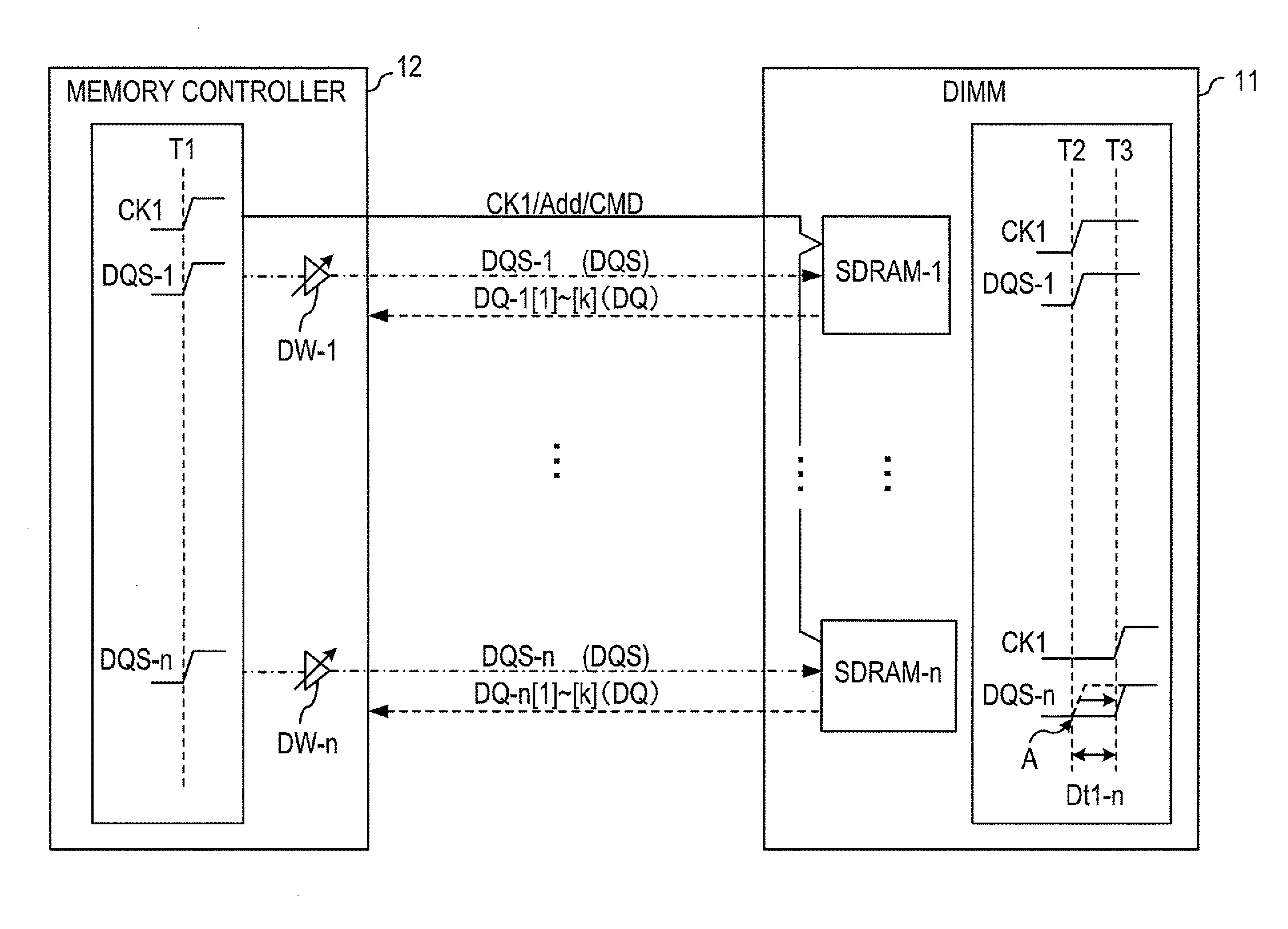
[0052]FIG. 4 is a diagram showing an example of the construction of an information processing device according to a first embodiment. FIG. 5 is a diagram showing an example of the circuit construction of a memory controller corresponding to SDRAM-1. FIG. 6 is a diagram showing an example of the circuit construction of a memory controller corresponding to SDRAM-n.

[0053]As a shown in FIG. 4, an information processing device (delay time control device) according to the first embodiment is constructed as a computer having DIMM (Dual Inline Memory Module) 11, a memory controller (memory control circuit) 12 and CPU (Central Processing Unit) 13.

[0054]DIMM 11 is a memory module having plural memories mounted therein. A DIMM 11 is constructed by plural (n; n represents a natural number of 2 or more) SDRAM (Synchronous DRAM; memory)-1 to SDRAM-n in this embodiment) as shown in FIG. 4. Furthermore, n represents the number of ch (channels) and it is represented by...

second embodiment

Description of Second Embodiment

[0187]An information processing device 10b according to a second embodiment will be described with reference to FIGS. 14 and 15.

[0188]FIG. 14 is a circuit diagram showing a part corresponding to SDRAM-1 of the memory controller in the information processing device according to this embodiment. FIG. 15 is a circuit diagram showing a part corresponding to SDRAM-n. FIG. 16 is a diagram showing the function of a third variable delay circuit.

[0189]As shown in FIGS. 14 and 15, the information processing device 10b as this embodiment is equipped with a third variable delay circuit DWR0 in place of the first variable delay circuit DW0 provided to each of the control circuit units 15-1 to 15-n of the first embodiment, a third variable delay circuit (variable delay circuit) DWR1 in place of the first variable delay circuit DW1 and the second variable delay circuit DR1 provided to each of the control circuit units 15-1 to 15-n of the first embodiment, and a thir...


PUM


Abstract

Variable delay circuit constructed by connecting plural unit circuits in series which can change a delay time from input of signal until output of the signal by increasing or decreasing the number of unit circuits through which the signal concerned is passed. Each of the unit circuits is operable in a through operation mode in which a signal input from a unit circuit at the front stage is output to a unit circuit at the rear stage and also a signal input from a unit circuit at the rear stage is output to a unit circuit at the front stage and a feedback operation mode in which a signal input from a unit circuit at the front stage to a unit circuit at the front stage and a signal input from a unit circuit at the rear stage is output to a unit circuit at the rear stage.

Description

CROSS-REFERENCE TO RELATED APPLICATIONS[0001]This application is related to and claims priority to Japanese patent application no. 2007-241611 filed on Sep. 18, 2007, in the Japan Patent Office, and incorporated by reference herein.BACKGROUND[0002]1. Field[0003]The circuit relates to a technique of setting a delay time from the input time of a signal until the output time of the signal.[0004]2. Description of the Related Art[0005]The speed of memory interfaces has increased year by year as memory interfaces have been recently developed. An example is the DDR 3 (Double Data Rate 3) memory interface, etc. which is standardized in JEDEC (Joint Electron Device Engineering Council).[0006]A DLL (Delay Locked Loop) is indispensable when such a memory interface is designed. A variable delay circuit that can change the delay time from input of a signal to output of the signal is used in the DLL (for example, see JP-A-2005-286467).[0007]Means for implementing the variable delay circuit is rou...

Claims


Application Information

Patent Timeline
Patent Type & Authority Applications(United States)
IPC IPC(8): H03L7/06G11C11/407G11C11/4076H03K5/13H03K5/131H03K5/14
CPCG11C7/22G11C7/222H03K5/133H03K2005/00058H03L7/0814H03K5/135G11C11/407G11C11/4093G11C11/4096
Inventor TOKUHIRO, NORIYUKI
Owner FUJITSU LTD
Features
  • R&D
  • Intellectual Property
  • Life Sciences
  • Materials
  • Tech Scout
  • Unparalleled Data Quality
  • Higher Quality Content
  • 60% Fewer Hallucinations
Learn More