Vertical group iii-nitride light emitting device and method for manufacturing the same

a technology of light-emitting devices and nitride, which is applied in semiconductor devices, in situ pavings, roads, etc., can solve the problems of extinction of light resulting from total internal reflection, and low external extraction efficiency, so as to improve light extraction efficiency and operating voltage properties.

Active Publication Date: 2009-03-19
SAMSUNG ELECTRONICS CO LTD
View PDF16 Cites 27 Cited by
  • Summary
  • Abstract
  • Description
  • Claims
  • Application Information

AI Technical Summary

Benefits of technology

[0011]The present invention has been made to solve the foregoing problems of the prior art and it is therefore an object of the present invention to provide a group III-nitride light emitting device considerably improved in light extraction efficiency and operating voltage properties.
[0012]It is another object of the invention to provide a method for manufacturing a vertical group III-nitride light emitting device having high extraction efficiency of light in an easy and simple fashion at a greater yield.

Problems solved by technology

Most of all, the biggest problem concerns low external extraction efficiency, that is, light generated is externally extracted at a low efficiency.
The greatest hurdle against light extraction out of the LED is extinction of light resulting from total internal reflection.
This increases a heat release rate of the LED, and decreases external extraction efficiency of the LED, thus shortening lifetime thereof.
Accordingly, current concentrates in a lower part of the n-electrode 18, disadvantageously increasing operating voltage Vf of the light emitting device 10.
However, with the sapphire substrate removed, it is very difficult to perform the photolithography on a top surface of a thin-filmed GaN-based structure having a thickness of 10 μm or less, even though the conductive substrate 11 is used as a supporting substrate.
Accordingly, this leads to significant decrease in yield.

Method used


Image

  • Vertical group iii-nitride light emitting device and method for manufacturing the same
  • Vertical group iii-nitride light emitting device and method for manufacturing the same
  • Vertical group iii-nitride light emitting device and method for manufacturing the same

Examples


Embodiment Construction

[0045]The present invention now will be described more fully hereinafter with reference to the accompanying drawings, in which preferred embodiments of the invention are shown. This invention, however, may be embodied in many different forms and should not be construed as limited to the embodiments set forth herein. Rather, these embodiments are provided so that this disclosure will be thorough and complete, and will fully convey the scope of the invention to those skilled in the art. In the drawings, the shapes and dimensions may be exaggerated for clarity, and the same reference signals are used to designate the same or similar components throughout.

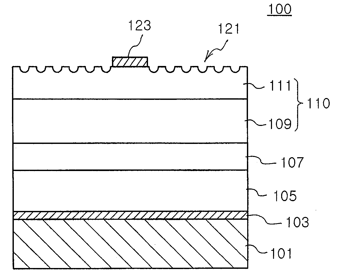
[0046]FIG. 2 is a side sectional view illustrating a vertical group III-nitride light emitting device according to one embodiment of the invention. Referring to FIG. 2, the light emitting device 100 includes a reflective layer 103, a p-type clad layer 105, an active layer 107, an n-doped AlxGayIn1-x-yN (0≦x≦1, 0≦y≦1, 0≦x+y≦1) layer 109...


PUM


Abstract

A vertical group III-nitride light emitting device and a manufacturing method thereof are provided. The light emitting device comprises: a conductive substrate; a p-type clad layer stacked on the conductive substrate; an active layer stacked on the p-type clad layer; an n-doped AlxGayIn1-x-yN layer stacked on the active layer; an undoped GaN layer stacked on the n-doped layer; and an n-electrode formed on the undoped GaN layer. The undoped GaN layer has a rough pattern formed on a top surface thereof.

Description

RELATED APPLICATION[0001]This application claims the benefit of Korean Patent Application No. 2005-29044 filed on Apr. 7, 2005 in the Korean Intellectual Property Office, the disclosure of which is incorporated herein by reference.BACKGROUND OF THE INVENTION[0002]1. Field of the Invention[0003]The present invention relates to a group III-nitride light emitting device and a manufacturing method thereof. More particularly, the present invention relates to a vertical group III-nitride light emitting device improved in light extraction efficiency, and a manufacturing method thereof.[0004]2. Description of the Related Art[0005]Since development of a light emitting diode (LED) including a group III-nitride semiconductor, it has been utilized as a light source in a variety of areas such as a liquid crystal display (LCD) backlight, a mobile phone keypad, a illumination lighting source and the like. Regarding development of the LED for wide-ranging purposes, light-emitting efficiency and hea...

Claims


Application Information

Patent Timeline
Patent Type & Authority Applications(United States)
IPC IPC(8): H01L33/00H01L33/06H01L33/10H01L33/22H01L33/32H01L33/42
CPCH01L33/0079H01L33/32H01L33/22H01L33/0093E01C7/06E01C7/35
Inventor LEE, JAE HOONKIM, YONG CHUNBACK, HYUNG KYKONG, MOON HEONKIM, DONG WOO
Owner SAMSUNG ELECTRONICS CO LTD
Why Eureka
Try Eureka