

JFET With Built In Back Gate in Either SOI or Bulk Silicon
a back gate and silicon technology, applied in the field of semiconductor devices, can solve the problems of reducing the overall total number of devices that can be formed on any wafer, consuming chip area, etc., and achieve the effect of reducing the disadvantages and eliminating the problems of prior jfets
- Summary
- Abstract
- Description
- Claims
- Application Information
AI Technical Summary
Benefits of technology
Problems solved by technology
Method used
Image

Examples
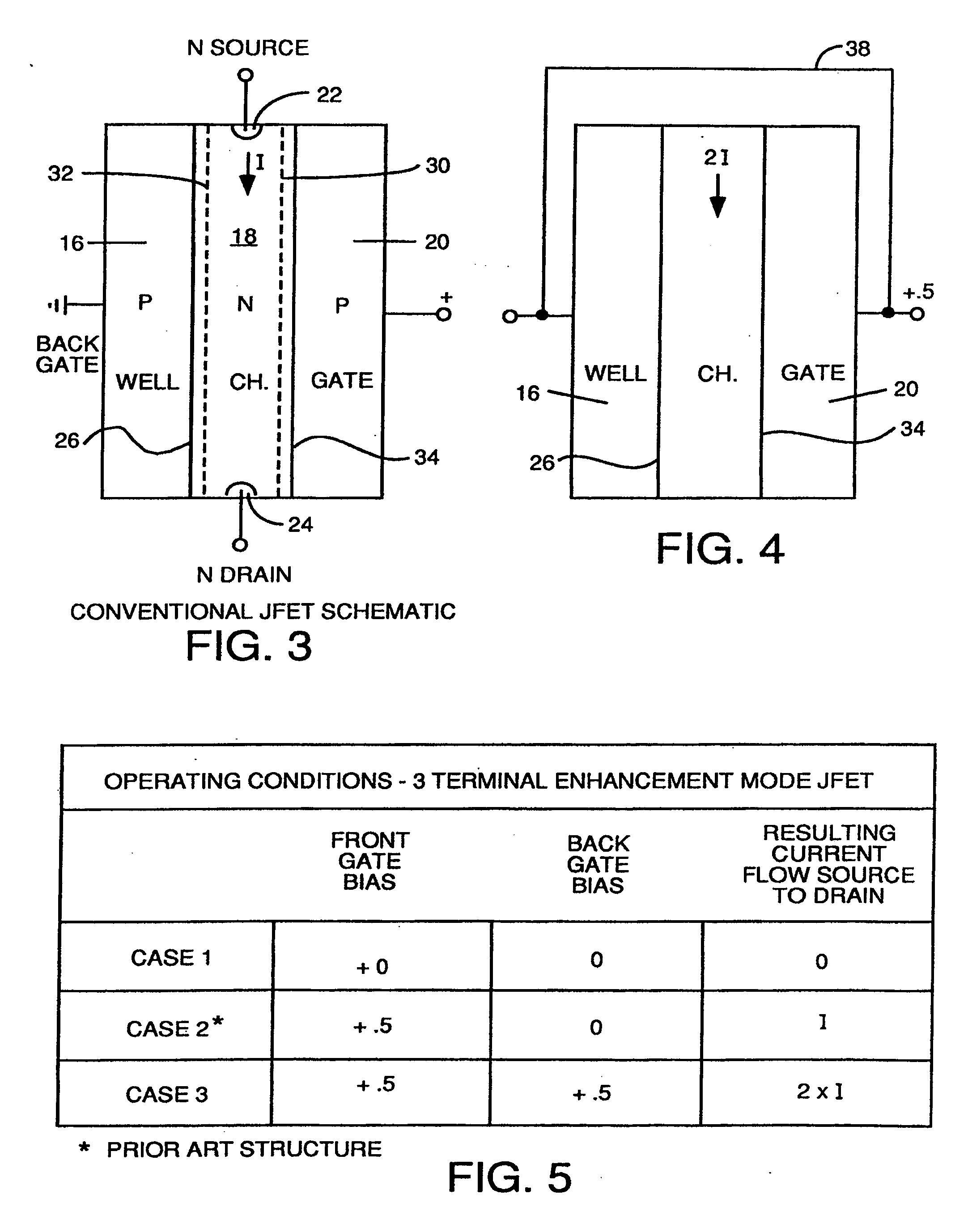
case 2
[0042 represents the prior art case shown in FIG. 3 where +0.5 volts is applied to the front gate and the back gate is grounded. In this case, source-to-drain current flow is i.
case 3
[0043 is the case according to the teachings of the invention where when +0.5 volts is applied to the front gate, the same bias of +0.5 is automatically applied to the back gate. This case is represented by FIG. 4. This case results in a source-to-drain current flow of 2 times i. The reason the current flow is 2i in Case 3 is because both the front gate and the back gate are forward biased. This causes the depletion region to pull back or disappear around both of junctions 26 and 34. This effectively doubles the volume in the channel through which current can flow and reduces the resistance proportionately. This increases the current flow to twice the level of the prior art when the back gate is grounded. Of course a current flow of 2i can be achieved in the prior art structure by using the surface contact of the back gate to forward bias the back gate junction.
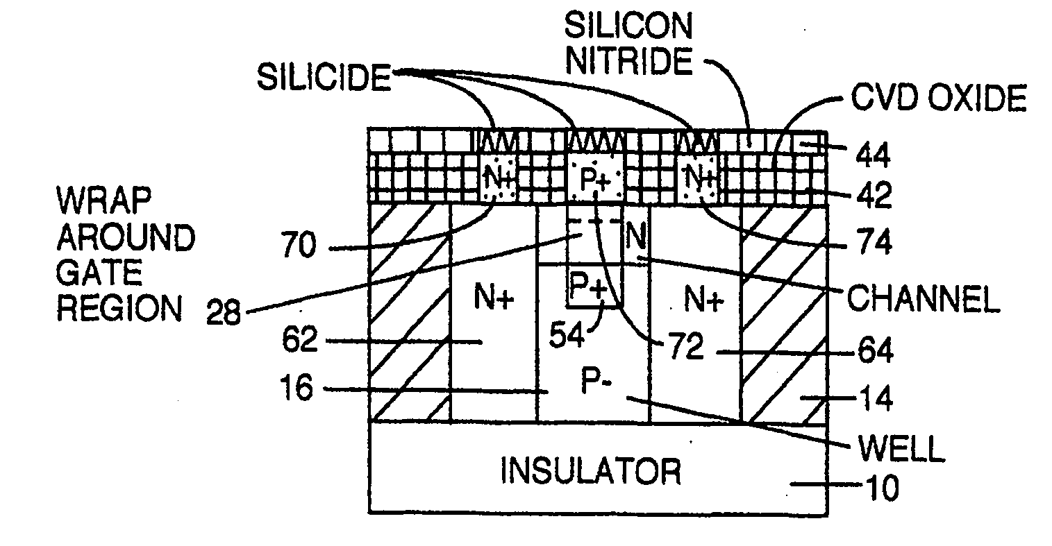
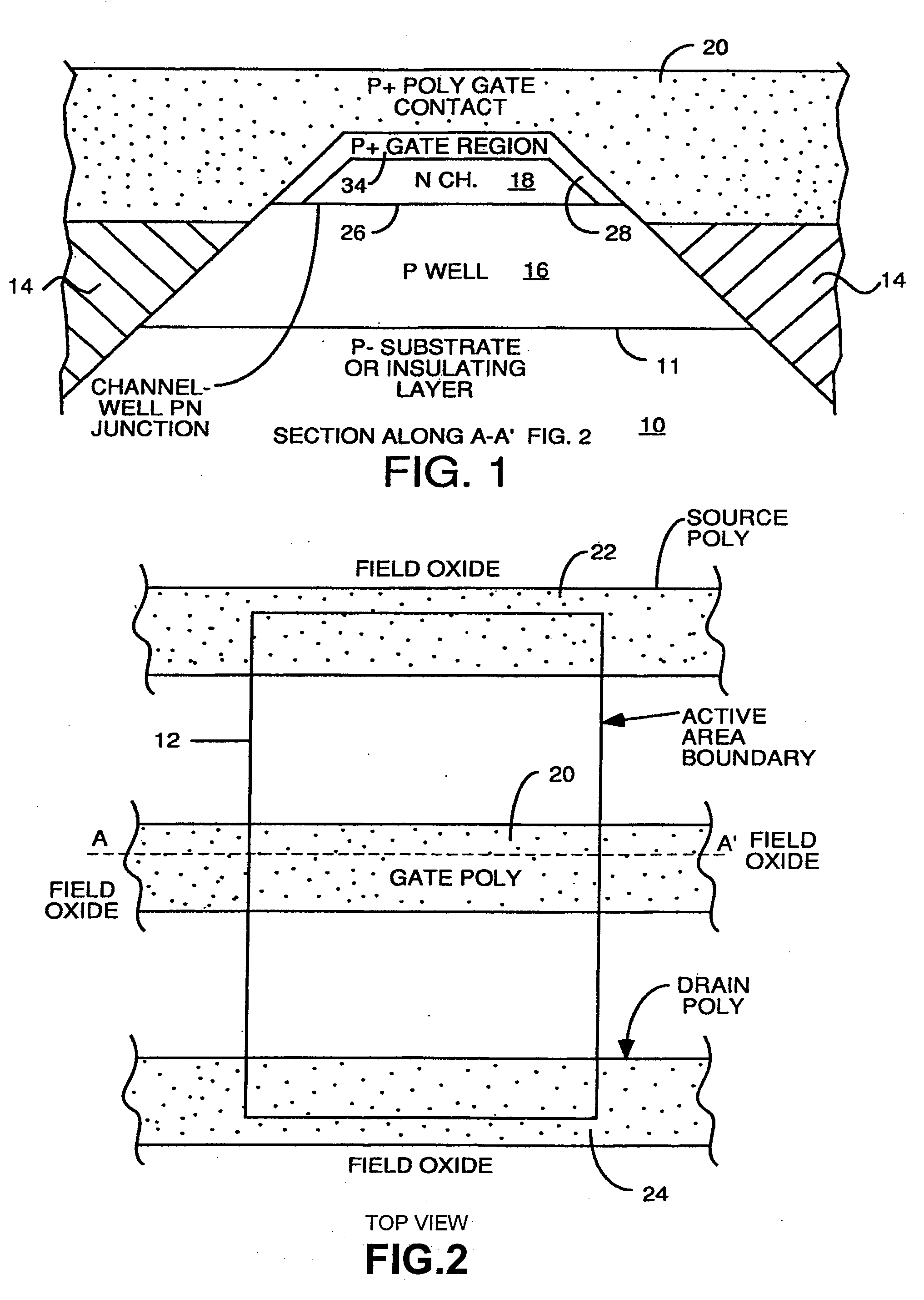
[0044]Appendix A is a table giving the process steps to construct the preferred embodiment, the step number and the figure ...
PUM
 Abstract
Description
Claims
Application Information