Camera module, manufacturing method of imaging apparatus and hot melt molding method

a technology of camera module and manufacturing method, applied in the field of camera module, can solve the problems of reducing productivity, unable to arrange electronic parts and patterns in a region of the circuit board, etc., and achieve the effect of reducing material cost and improving productivity

Inactive Publication Date: 2009-03-26
HITACHT MAXELL LTD
View PDF8 Cites 73 Cited by
  • Summary
  • Abstract
  • Description
  • Claims
  • Application Information

AI Technical Summary

Benefits of technology

[0011]The present invention is made for solving the technical object mentioned above. In other words, an object of the present invention is to provide a camera module which can make a work for filling up a clearance between a pedestal mount and a circuit board in a post process unnecessary, can conduct a shield portion with a circuit board at a time of a reflow heating, and can intend to improve a productivity and reduce a material cost.
[0012]An object of the present invention is to provide a camera module and a hot melt molding method which can make a work for filling up a clearance between a pedestal mount and a circuit board in a post process, and can achieve a downsizing by reducing a protruding portion of an adhesive agent or the like.
[0033]In accordance with the present invention, there is provided a camera module including a lens unit, an imaging element converting an incoming light formed by the lens unit into an electric signal, and a pedestal mount having a side wall portion defining a space storing the imaging element and to which the lens unit is attached, wherein the pedestal mount is provided with a hot melt portion formed in the side wall portion, molten at a reflow temperature so as to be used for adhering with a board and made of a thermoplastic resin, and an outer surface groove portion formed in an outer surface of the side wall portion and formed in such a manner that an area of a lower surface of the side wall portion adhered to the board is partly decreased.
[0035]In accordance with the present invention, there is provided a hot melt molding method of forming a hot melt portion made of a thermoplastic resin on a lower surface of a side wall portion of a pedestal mount to which a lens and an imaging element converting an incoming light formed by the lens into an electric signal are attached, by using an injection molding metal mold, including the steps of installing the pedestal mount in the injection molding metal mold in such a manner that a groove portion formed on an outer surface of the side wall portion is positioned at an injection port of the injection molding metal mold so as to partly decrease an area of the lower surface of the pedestal mount, injecting the thermoplastic resin in a molten state from the injection port, and picking up the pedestal mount from the injection molding metal mold after the thermoplastic resin is hardened.
[0037]In accordance with the present invention, the work for filling up the clearance between the pedestal mount and the circuit board in the post process is not necessary, and it is possible to achieve a downsizing by decreasing the protruding portion of the adhesive agent or the like.

Problems solved by technology

However, since a work for filling up the clearance mentioned above is generally carried out after a reflow soldering process heating the circuit board mounting the camera module thereon by a predetermined heating furnace (a reflow furnace), a process of operation is increased, and the work causes a reduction in a productivity.
Further, if the adhesive agent or the like for filling up the clearance is expanded on the circuit board, and runs over largely to an outer side from the pedestal mount, it is impossible to arrange electronic parts and patterns in a region of the circuit board in which the adhesive agent or the like runs over.

Method used


Image

  • Camera module, manufacturing method of imaging apparatus and hot melt molding method
  • Camera module, manufacturing method of imaging apparatus and hot melt molding method
  • Camera module, manufacturing method of imaging apparatus and hot melt molding method

Examples


first embodiment

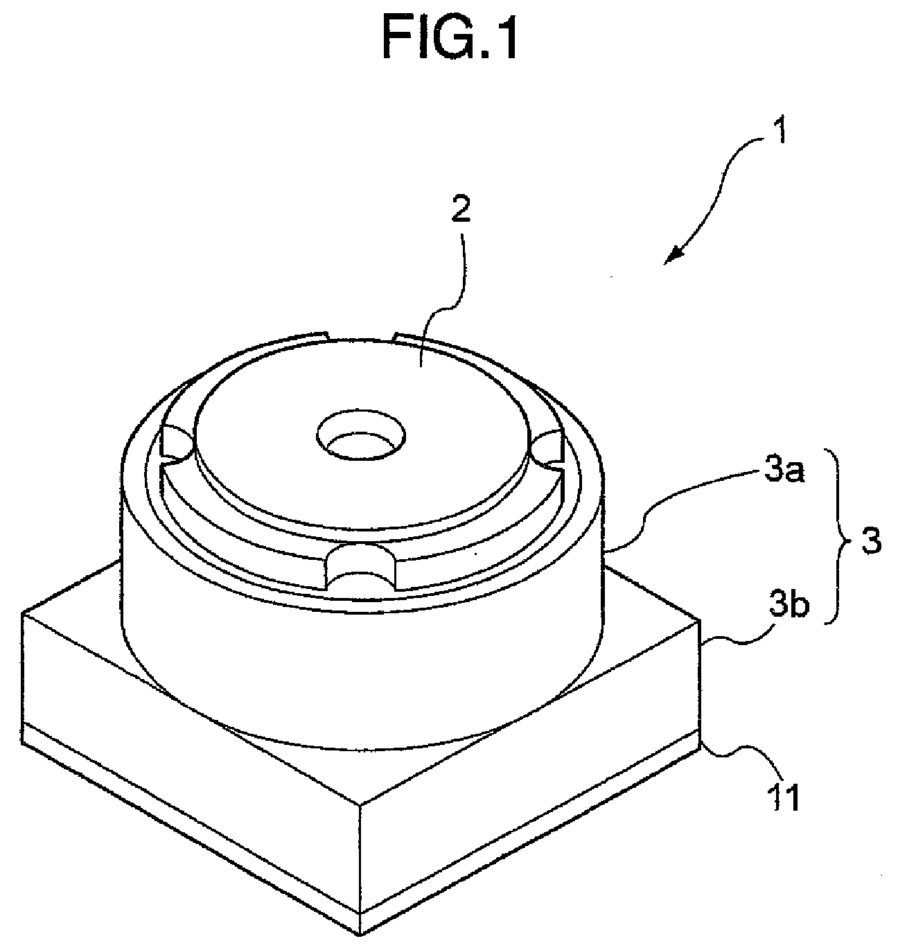
[0057]FIG. 1 is a view explaining a camera module 1 to which the present embodiment (a first embodiment) is applied. As shown in FIG. 1, the camera module 1 is provided with a lens unit 2 retaining a plurality of lenses (mentioned below), and a pedestal mount 3 mounting the lens unit 2. The pedestal mount 3 has a cylinder portion 3a to which the lens unit 2 is mounted, and a rectangular portion 3b integrally structured with the cylinder portion 3a, and a bottom surface portion 11 constituted by a thermoplastic resin is provided in a lower end of the rectangular portion 3b of the pedestal mount 3. The bottom surface portion 11 will be described later. In this case, a part obtained by attaching the lens unit 2 to the pedestal mount 3 may be called as a body tube.

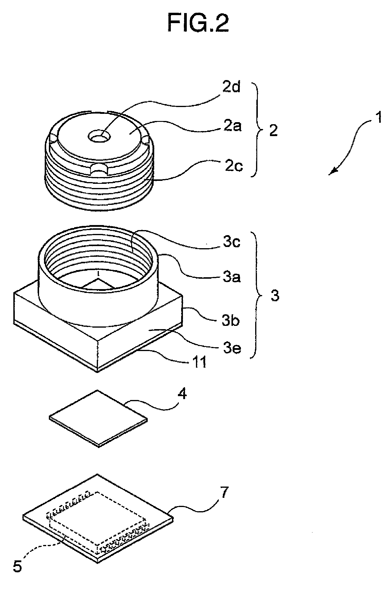
[0058]FIG. 2 is an exploded perspective view of the camera module 1 shown in FIG. 1. As shown in FIG. 2, the camera module 1 is provided with the lens unit 2 and the pedestal mount 3. Further, the camera module 1 is provided w...

second embodiment

[0091]In this case, in the present embodiment, the description is given of the case that the predetermined clearance C is provided between the bottom surface portion 11 and the circuit board (not shown), as shown in FIG. 3, however, the present invention can be applied to a case that the clearance C is not provided.

[0092]FIG. 6 is a vertical cross sectional view of a second embodiment of the camera module. FIGS. 6A and 6B show vertical cross sectional views of a lower portion from the rectangular portion 3b of the pedestal mount 3 constructing the camera module, and the cylinder portion 3a and the lens unit 2 are omitted. In this case, the same reference numerals are attached to the same structure as the camera module 1 shown in FIG. 3, and a description thereof will be omitted.

[0093]As shown in FIG. 6A, the bottom surface portion 11 made of the thermoplastic resin is provided in the lower end of the side wall portion 3e constructing the rectangular portion 3b of the pedestal mount ...

third embodiment

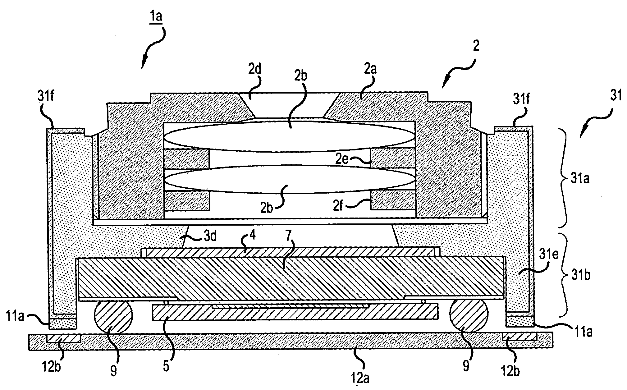
[0107]FIG. 7 is a vertical cross sectional view of a third embodiment of the camera module. The same reference numerals are attached to the same structures as those of the camera module 1 shown in FIG. 3, and a description thereof will be omitted.

[0108]The camera module 1a shown in FIG. 7 is structured such that a conductive membrane 31f is formed in a surface of a side wall portion 31e of a pedestal mount 31 (cylinder portion 31a and a rectangular portion 31b, and a whole is electromagnetically shielded.

[0109]Further, a bottom surface portion 11a is provided in a lower end of the side wall portion 31e of the pedestal mount 31 so as to be integrally formed with the side wall portion 31e. In this case, the bottom surface portion 11a is constructed by a thermoplastic resin composition including a thermoplastic resin melting at a reflow temperature and a conductive filler.

[0110]As shown in FIG. 7, the bottom surface portion 11a forms a predetermined clearance between the pedestal mount...


PUM


Abstract

The invention provides a camera module which can make a work for filling up a clearance between a pedestal mount and a circuit board in a post process unnecessary. The invention provides a camera module including a lens unit, an imaging element converting an incoming light formed by the lens unit into an electric signal and a pedestal mount attaching the lens unit thereto and storing the imaging element, in which a lower end portion of a side wall portion of the pedestal mount is provided with a bottom surface portion made of a thermoplastic resin melting at a reflow temperature.

Description

BACKGROUND OF THE INVENTION[0001](1) Field of the Invention[0002]The present invention relates to a cameral module or the like, and more particularly to a camera module or the like, for example, mounted to a cellular phone or the like.[0003](2) Description of Related Art[0004]In recent years, a camera system is mounted to various devices such as a cellular phone or the like. A camera module forming a subject image on an image sensor by using a micro lens is widely used in the camera system mentioned above.[0005]With regard to the camera module mentioned above, for example, patent document 1 (JP-A-2004-304604) describes that a reliability of an electric connection between a compact camera module and a socket is improved by setting an attaching structure of the compact camera module to the socket such as to prevent a spring-like arm portion of the socket from coming into contact with the compact camera module.[0006]In the case of a camera module using a package sensor in which an imag...

Claims


Application Information

Patent Timeline
Patent Type & Authority Applications(United States)
IPC IPC(8): H04N5/225
CPCG02B7/021G02B13/001H04N5/2257H04N5/2253H04N5/2254G03B17/00H04N23/52H04N23/54H04N23/57H04N23/55
Inventor AOKI, SUSUMUHASUDA, TAKASHI
Owner HITACHT MAXELL LTD
Why Eureka
Try Eureka