Method and apparatus for controlling dual conversion gain signal in imaging devices

a technology of dual conversion gain and control scheme, which is applied in the field of dual conversion gain control scheme of imaging devices, can solve the problems of insufficient conversion gain time and reliability problems

Active Publication Date: 2009-04-16
SEMICON COMPONENTS IND LLC
View PDF4 Cites 26 Cited by
  • Summary
  • Abstract
  • Description
  • Claims
  • Application Information

AI Technical Summary

Problems solved by technology

However, as will be explained in more detail below, this scheme tends to result in the problem of insufficient time for the conversion gain to fully settle to the second value from the first value.
Although this scheme solves the issue with insufficient settling time, it tends to result in reliability issue in the form of degradation of the gate oxide layer of the dual conversion gain transistors due to high stress.

Method used


Image

  • Method and apparatus for controlling dual conversion gain signal in imaging devices
  • Method and apparatus for controlling dual conversion gain signal in imaging devices
  • Method and apparatus for controlling dual conversion gain signal in imaging devices

Examples


Embodiment Construction

[0013]Certain details are set forth below to provide a sufficient understanding of embodiments of the invention. However, it will be clear to one skilled in the art that embodiments of the invention may be practiced without these particular details. Moreover, the particular embodiments of the present invention described herein are provided by way of example and should not be used to limit the scope of the invention to these particular embodiments. In other instances, well-known circuits, control signals, and timing protocols have not been shown in detail in order to avoid unnecessarily obscuring the invention.

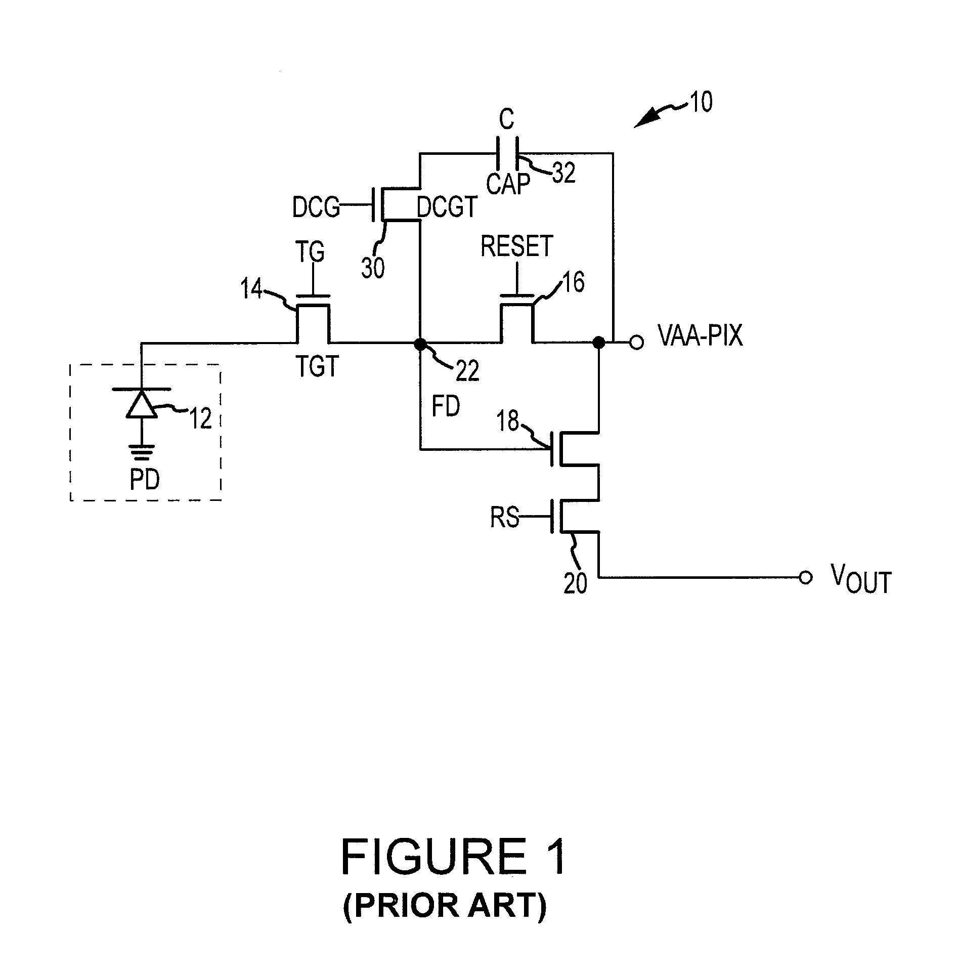
[0014]FIG. 1 illustrates a schematic diagram of an example of a prior art dual conversion gain-enabled pixel cell 10 of an imaging device. Similar to most four-transistor (4T) pixels, the pixel cell 10 includes a photosensor 12 (PD), floating diffusion node 22 (FD), transfer transistor 14 (TGT), reset transistor 16, source follower transistor 18, and row select transistor 20. I...


PUM


Abstract

A image-sensing device includes an array of light-sensing pixels arranged in rows, a readout circuit, and a control logic coupled to the rows of pixels. Each of the pixels has a respective conversion gain that changes to a respective second value from a respective first value within a settling time when a control signal is applied to the pixel. The readout circuit is coupled to the array of pixels and samples the rows of pixels once in an array sampling process. The control logic applies the control signal to the pixels of at least one row after sampling of the pixels in at least one other row of the array has begun but at least the settling time before the at least one row is sampled.

Description

TECHNICAL FIELD[0001]Embodiments of the present invention relate generally to imaging devices, and, more particularly, to dual conversion gain control scheme for imaging devices.BACKGROUND OF THE INVENTION[0002]Imaging devices, including charge coupled devices (CCD) and complementary metal-oxide-semiconductor (CMOS) imagers, are commonly used in image sensing applications such as digital cameras, video camcorders, scanners and the like. A prior art imager typically contains a focal plane array of light-sensing elements, referred to as picture elements or “pixels,” and readout circuitry that outputs signals indicative of the light sensed by the pixels. Each light-sensing element contains a photosensor that generates and accumulates photo-generated charge proportional to the amount of the incident light striking the surface of the light-sensing element. That is, the photosensor converts the incoming light photons to an electrical signal in the form of electric charge. Moreover, the se...

Claims


Application Information

Patent Timeline
Patent Type & Authority Applications(United States)
IPC IPC(8): H04N5/235H04N5/228H04N5/335H04N5/355H04N5/3745
CPCH04N3/155H04N5/37452H04N5/3559H04N25/59H04N25/771
Inventor LI, XIANGLI
Owner SEMICON COMPONENTS IND LLC
Why Eureka
Try Eureka