

Radiation image converting panel, scintillator panel and radiation image sensor
- Summary
- Abstract
- Description
- Claims
- Application Information
AI Technical Summary
Benefits of technology
Problems solved by technology
Method used
Image

Examples
Embodiment Construction
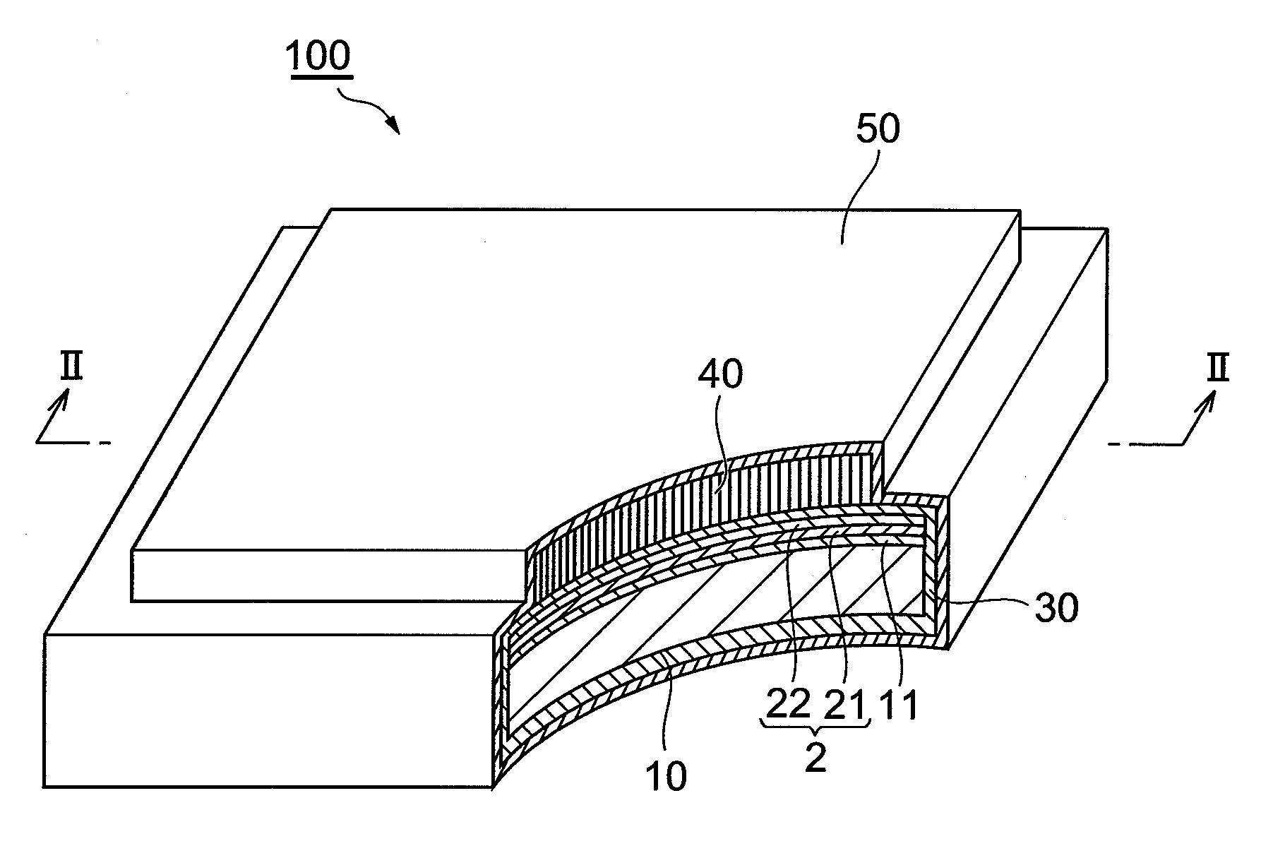
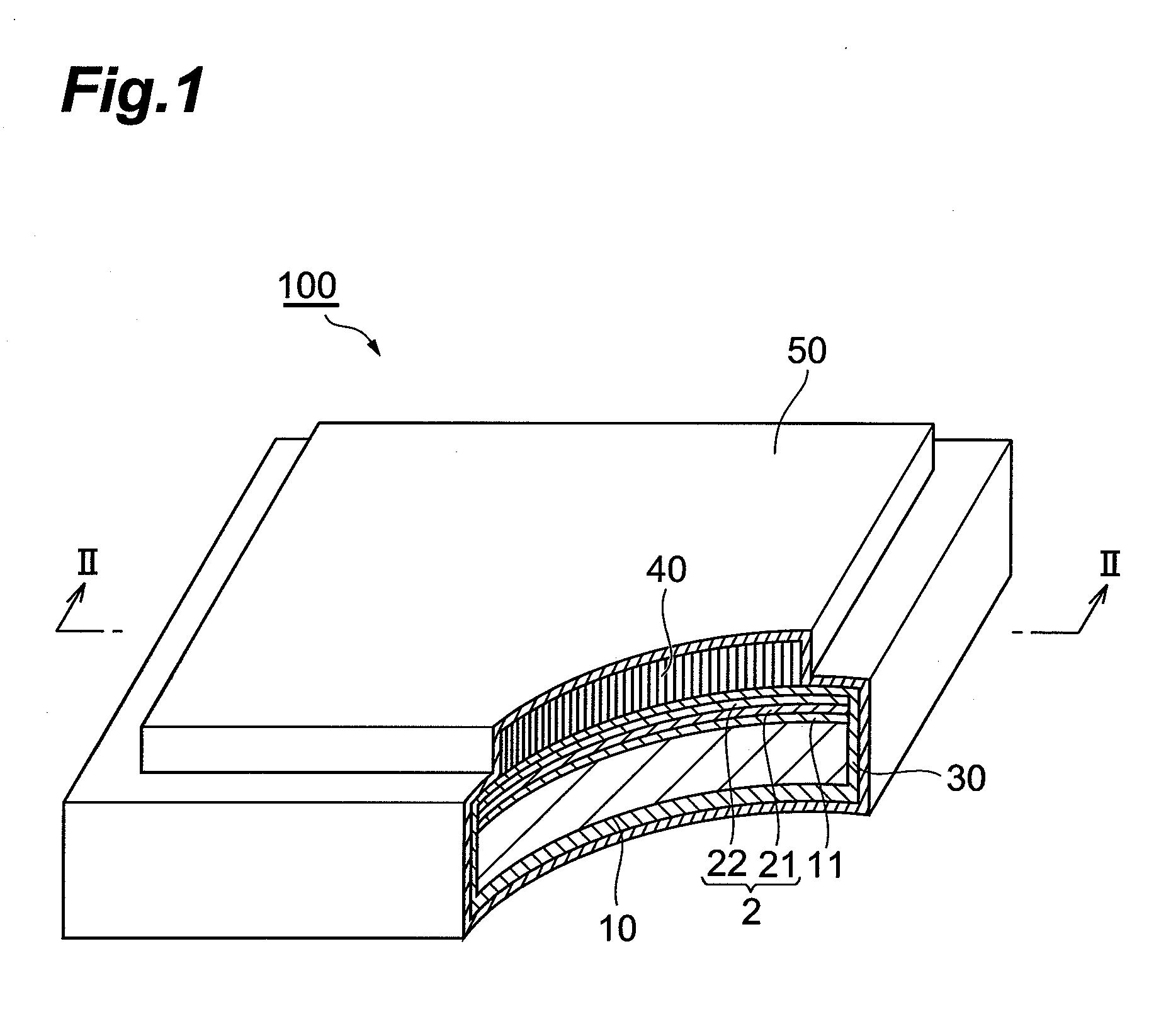
[0030]Hereinafter, preferred embodiments of the present invention will be described in detail with reference to the accompanying drawings. To facilitate the comprehension of the explanation, the same reference numerals denote the same parts, where possible, throughout the drawings, and a repeated explanation will be omitted. In addition, dimensions in the respective drawings have been overdrawn in part for the sake of description, and are not always coincident with those in reality.
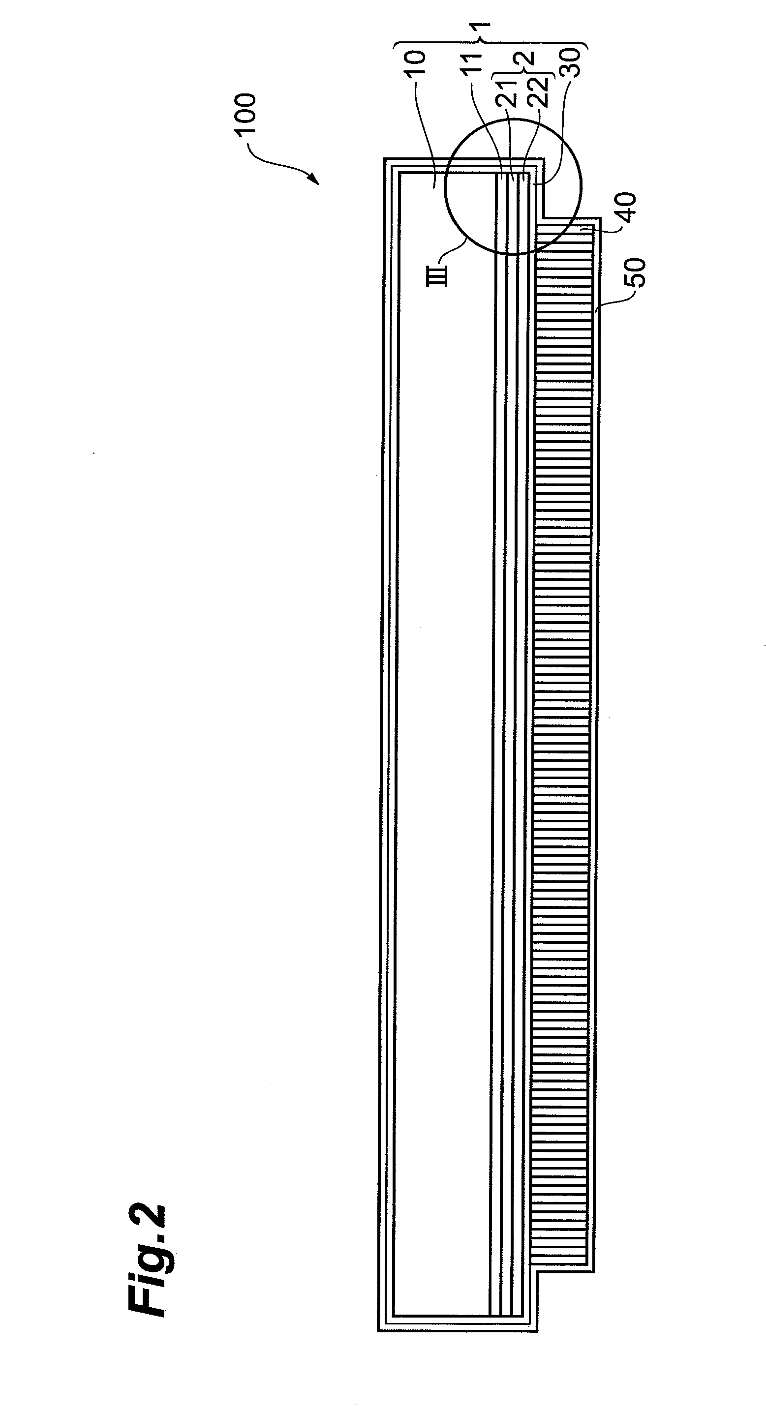
[0031]FIG. 1 to FIG. 3 show a configuration of a first embodiment of a radiation image converting panel according to the present invention. The present embodiment is a scintillator panel using a scintillator as a converting portion of a radiation image and is therefore also a preferred embodiment of a scintillator panel according to the present invention. FIG. 1 is a partially broken perspective view thereof, FIG. 2 is a sectional view along a line II-II thereof, and FIG. 3 is an enlarged view of a part I...
PUM
 Abstract
Description
Claims
Application Information