Liquid crystal display device

a liquid crystal display and display device technology, applied in non-linear optics, instruments, optics, etc., can solve the problems and affecting the brightness of liquid crystal display devices. , to achieve the effect of reducing the directivity of viewing angle characteristic, increasing transmissivity, and increasing the brightness of liquid crystal display devices

Active Publication Date: 2009-04-23
PANASONIC LIQUID CRYSTAL DISPLAY CO LTD +1
View PDF5 Cites 27 Cited by
  • Summary
  • Abstract
  • Description
  • Claims
  • Application Information

AI Technical Summary

Benefits of technology

[0035]According to the present invention, in the IPS liquid crystal display device having the TFT substrate on which the common electrode formed of the planar matted electrode and the comb-teeth-shaped pixel electrodes are arranged with the insulation film sandwiched between the common electrode and the pixel electrodes, the direction of the comb-teeth-shaped pixel electrode is reversed between an upper side and a lower side within the pixel thus reducing the directivity of viewing angle characteristic.
[0036]Further, the profile of the pixel electrode is formed in a laterally-extending trapezoidal shape and the pixel electrodes are arranged in a packed manner by changing the direction of the trapezoidal shape in the longitudinal direction, while a light blocking film is not arranged between the pixel electrodes in the longitudinal direction and hence, transmissivity is increased whereby brightness of the liquid crystal display device can be increased.
[0037]Further, on the counter substrate, the color filters are formed in a continuous stripe shape along the pixel electrodes thus forming the trapezoidal pixel electrodes and hence, possibility of color mixing can be reduced even when the packed structure is adopted. That is, by forming the color filters in a stripe shape in the longitudinal direction, it is possible to prevent color mixing even when the light blocking film is not formed between the pixel electrodes in the longitudinal direction.
[0038]Further, with respect to the light blocking films arranged in the lateral direction on the counter substrate, the light blocking films are formed only on portions which are inevitable for blocking light to TFTs or the like formed on the TFT substrate and the light blocking films are not formed on other portions thus increasing transmissivity.
[0039]As described above, according to the present invention, it is possible to realize the liquid crystal display device of high brightness which exhibits excellent viewing angle characteristic.

Problems solved by technology

In the IPS liquid crystal display device disclosed in patent document 1, the pixel electrodes and the common electrodes are formed on the same TFT substrate and hence, the liquid crystal display device basically has a drawback with respect to transmissivity.
Further, the increase of portions which do not contribute to a display in the vicinity of the scanning line is disadvantageous with respect to brightness.
Further, the constitution disclosed in patent document 2 is further disadvantageous compared to the constitution disclosed in patent document 1 in terms of transmissivity with respect to a point that the capacitive lines are formed.

Method used


Image

  • Liquid crystal display device
  • Liquid crystal display device
  • Liquid crystal display device

Examples


embodiment 1

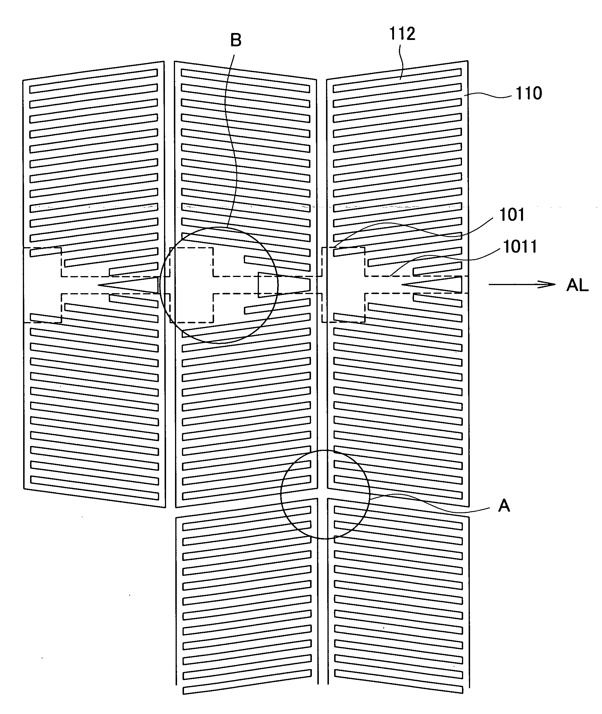
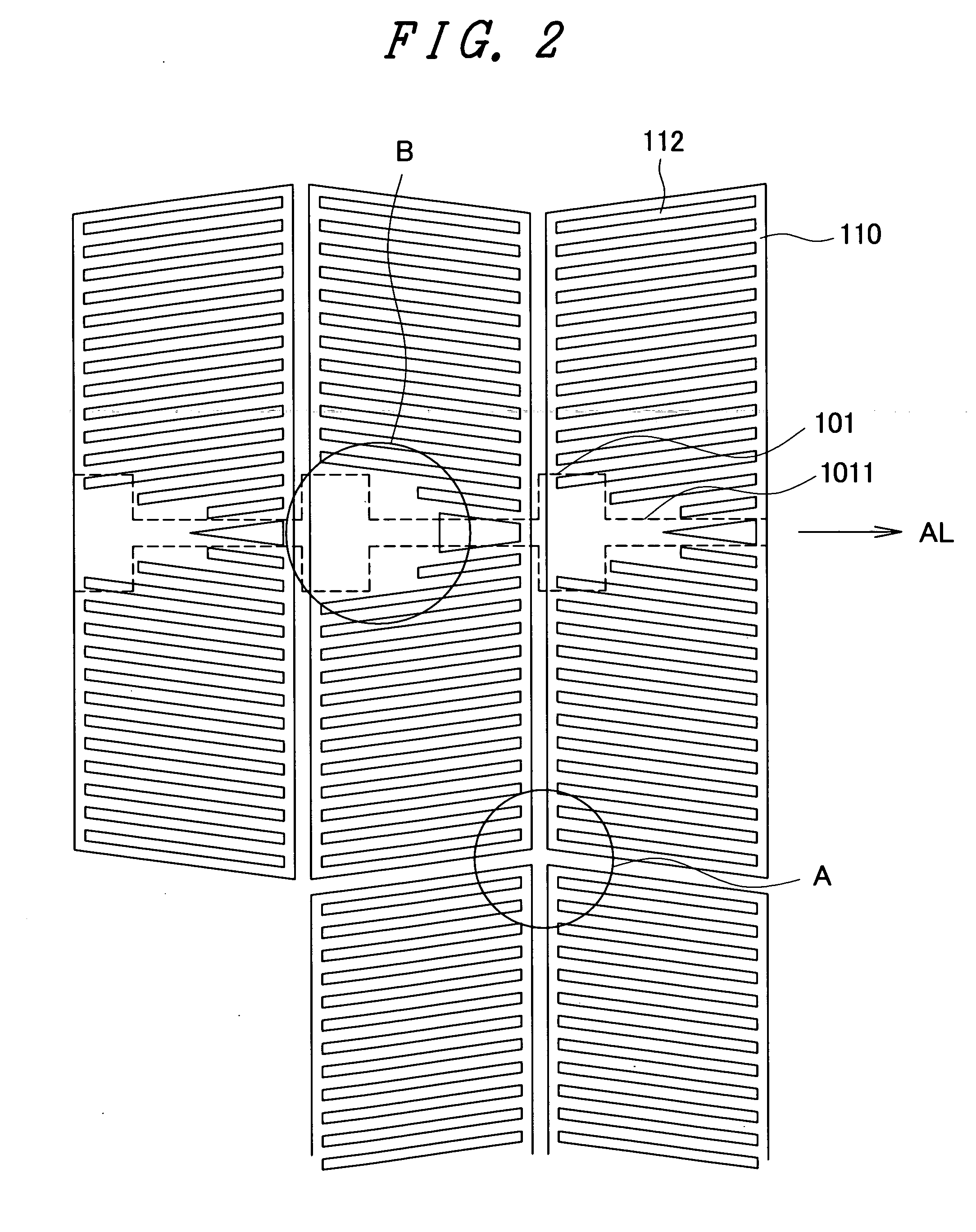
[0059]FIG. 2 is a plan view showing the arrangement of the pixels on the TFT substrate 100 of the embodiment 1. FIG. 3 is an enlarged plan view of a portion A which is a boundary portion of the pixel shown in FIG. 2. FIG. 4 is an enlarged view of a portion B which is the vicinity of the TFT in FIG. 2 in a see-through manner.

[0060]In FIG. 2, to prevent the drawing from becoming complicated, only the pixel electrodes 110 and the scanning line 1011 are shown. In FIG. 2, the pixel is formed in a laterally extending trapezoidal shape. Conventionally, the pixel is defined by a region surrounded by video signal lines and scanning lines. However, in this embodiment, the pixel is defined by the pixel electrode 110 per se. The pixels are arranged by alternately changing (reversing) the direction of the laterally extending trapezoidal shape in the longitudinal direction to have the packed structure.

[0061]Further, in this embodiment, the pixels are arranged by alternately changing (reversing) t...

embodiment 2

[0086]In the present invention, to increase the transmissivity as much as possible, an area where the scanning line 1011 (gate electrode 101) and the drain electrode 105 overlap with each other is increased. In this case, a capacitance Cgd between the gate electrode 101 and the drain electrode 105 is increased. When the capacitance Cgd is increased, a so-called voltage shift which is a phenomenon in which a voltage of the pixel electrode 110 is changed due to a change of the gate voltage is increased. Accordingly, it is preferable to set the capacitance Cgd to a small value. This embodiment is provided for setting the capacitance Cgd to a small value.

[0087]The pixel position in this embodiment is substantially equal to the pixel position shown in FIG. 2. However, this embodiment 2 differs from the embodiment 1 with respect to the structure of the portion B shown in FIG. 2. FIG. 6 is a plan view showing an example of the constitution which decreases a capacitance Cgd between a scanni...

embodiment 3

[0095]FIG. 10 is a plan view showing the arrangement of pixels on a TFT substrate 100 of the embodiment 3 of the present invention. FIG. 11 is an enlarged plan view of a portion A which is a boundary portion of the pixel shown in FIG. 10. In FIG. 10, to prevent the drawing from becoming complicated, only pixel electrodes 110 and scaling lines 1011 are described. In FIG. 10, the pixel is formed in a laterally extending trapezoidal shape. Also in this embodiment, in the same manner as the embodiment 1, the pixel is defined by the pixel electrode 110 per se. The pixels are arranged by alternately changing (reversing) the direction of the laterally extending trapezoidal shape in the longitudinal direction thus forming the packed structure.

[0096]On the other hand, the arrangement of pixels in the lateral direction of this embodiment differs from the corresponding pixel arrangement of the embodiment 1. In this embodiment 3, the pixels having a laterally extending trapezoidal shape are arr...


PUM

PropertyMeasurementUnit
thicknessaaaaaaaaaa
electric fieldaaaaaaaaaa
brightnessaaaaaaaaaa

Abstract

The present invention realizes an IPS liquid crystal display device which exhibits small directivity of viewing angle and high brightness. Below a pixel electrode having a comb-teeth-shaped electrode and having a laterally-extending trapezoidal profile, a planar common electrode not shown in the drawing is formed by way of an insulation film. When a video signal is applied to the pixel electrode, an electric field is generated between the pixel electrode and the common electrode via slit portions formed in the pixel electrode thus controlling liquid crystal molecules. The pixel electrodes are arranged in a packed state by alternately reversing the direction of the trapezoidal shape in the longitudinal direction. Since a light blocking film is not present between two pixel electrodes arranged adjacent to each other in the longitudinal direction, the liquid crystal display device can acquire high transmissivity. As a result, a liquid crystal display device having high brightness can be realized.

Description

[0001]The present application claims priority from Japanese application JP2007-273708 filed on Oct. 22, 2007, the content of which is hereby incorporated by reference into this application.BACKGROUND OF THE INVENTION[0002]1. Field of the Invention[0003]The present invention relates to a liquid crystal display device, and more particular to a lateral-electric-field liquid crystal display device which exhibits excellent viewing angle characteristic and brightness characteristic.[0004]2. Background Art[0005]A liquid crystal display device includes a TFT substrate on which pixel electrodes, thin film transistors (TFT) and the like are formed in a matrix array and a counter substrate which faces the TFT substrate in an opposed manner and forms color filters or the like thereon at places corresponding to the pixel electrodes, and liquid crystal is sandwiched between the TFT substrate and the counter substrate. Further, an image is formed by controlling transmissivity of light for every pi...

Claims


Application Information

Patent Timeline
Patent Type & Authority Applications(United States)
IPC IPC(8): G02F1/1343G02F1/1335
CPCG02F2201/40G02F1/134363
Inventor TANNO, JUNJIMORIMOTO, MASATERUSASAKI, TOHRU
Owner PANASONIC LIQUID CRYSTAL DISPLAY CO LTD
Why Eureka
Try Eureka