Semiconductor device

a semiconductor and device technology, applied in the field of semiconductor devices, can solve the problems of semiconductor devices degrading in quality and reliability, water entering chips, melting and volume expansion of diffusion layer conductive films, etc., and achieve the effect of preventing the generation of chipping defects

Inactive Publication Date: 2009-04-30
PANASONIC CORP
View PDF0 Cites 20 Cited by
  • Summary
  • Abstract
  • Description
  • Claims
  • Application Information

AI Technical Summary

Benefits of technology

[0044]As has been described above, in the semiconductor device of the invention, an interlayer insulating film can be uniformly removed by laser light in a dicing process of a semiconductor substrate (wafer) by a laser grooving method. Therefore, generation of chipping defects can be prevented.

Problems solved by technology

In the laser grooving method, when laser light transmits to a diffusion layer, the laser light is absorbed by a diffusion layer conductive film formed in the diffusion layer, causing melting and volume expansion of the diffusion layer conductive film.
Such peeling causes problems such as water entering chips, and chippings are also produced from the peeled part in a dicing process performed after the laser grooving process.
As a result, the semiconductor device is degraded in quality and reliability.

Method used


Image

  • Semiconductor device
  • Semiconductor device
  • Semiconductor device

Examples


first embodiment

[0068]A first embodiment of the invention will be described with reference to the figures.

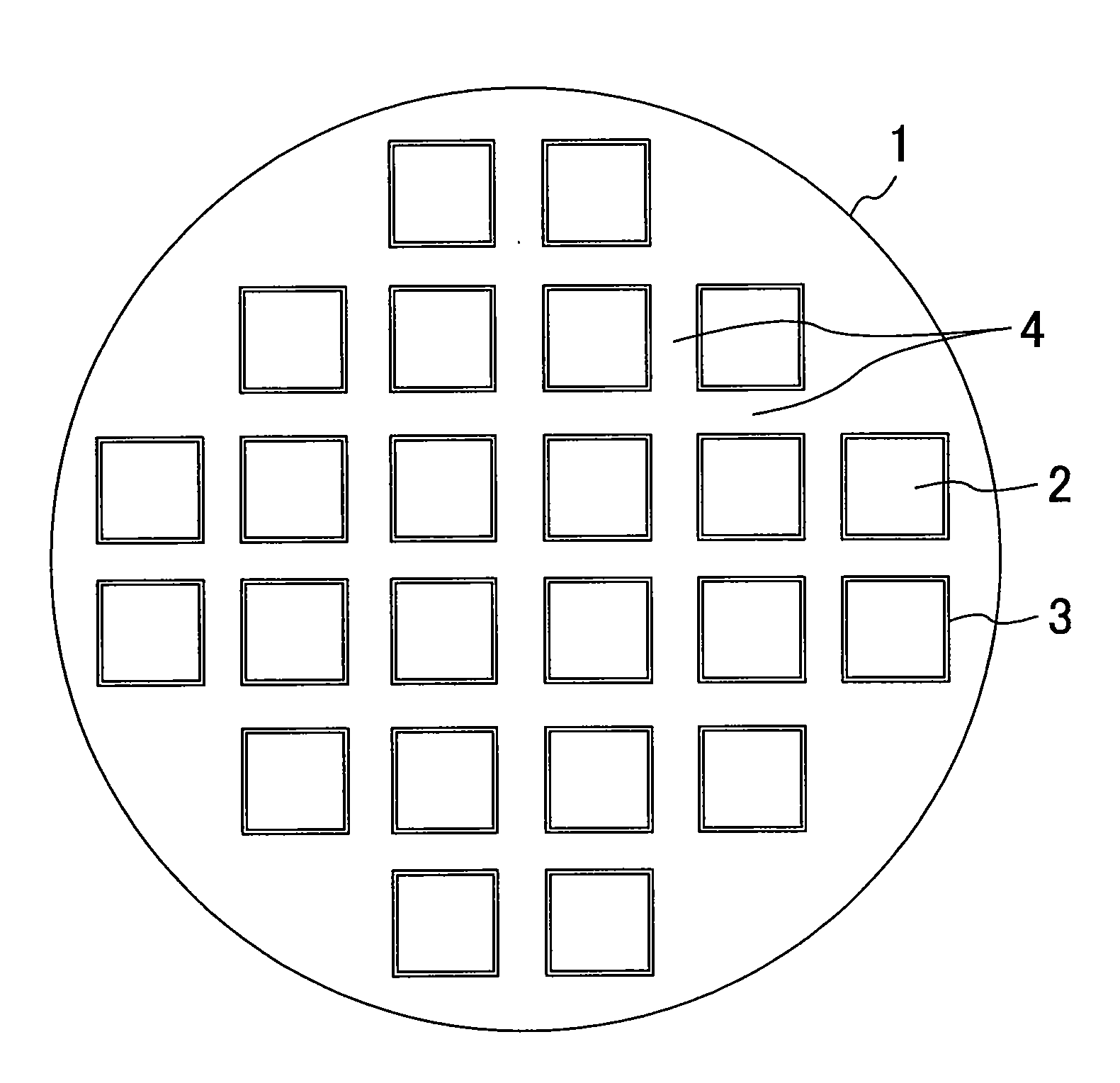
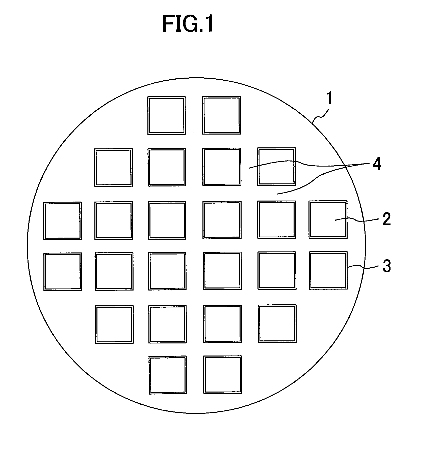
[0069]FIG. 1 is a plan view of a wafer-level semiconductor device according to the first embodiment.

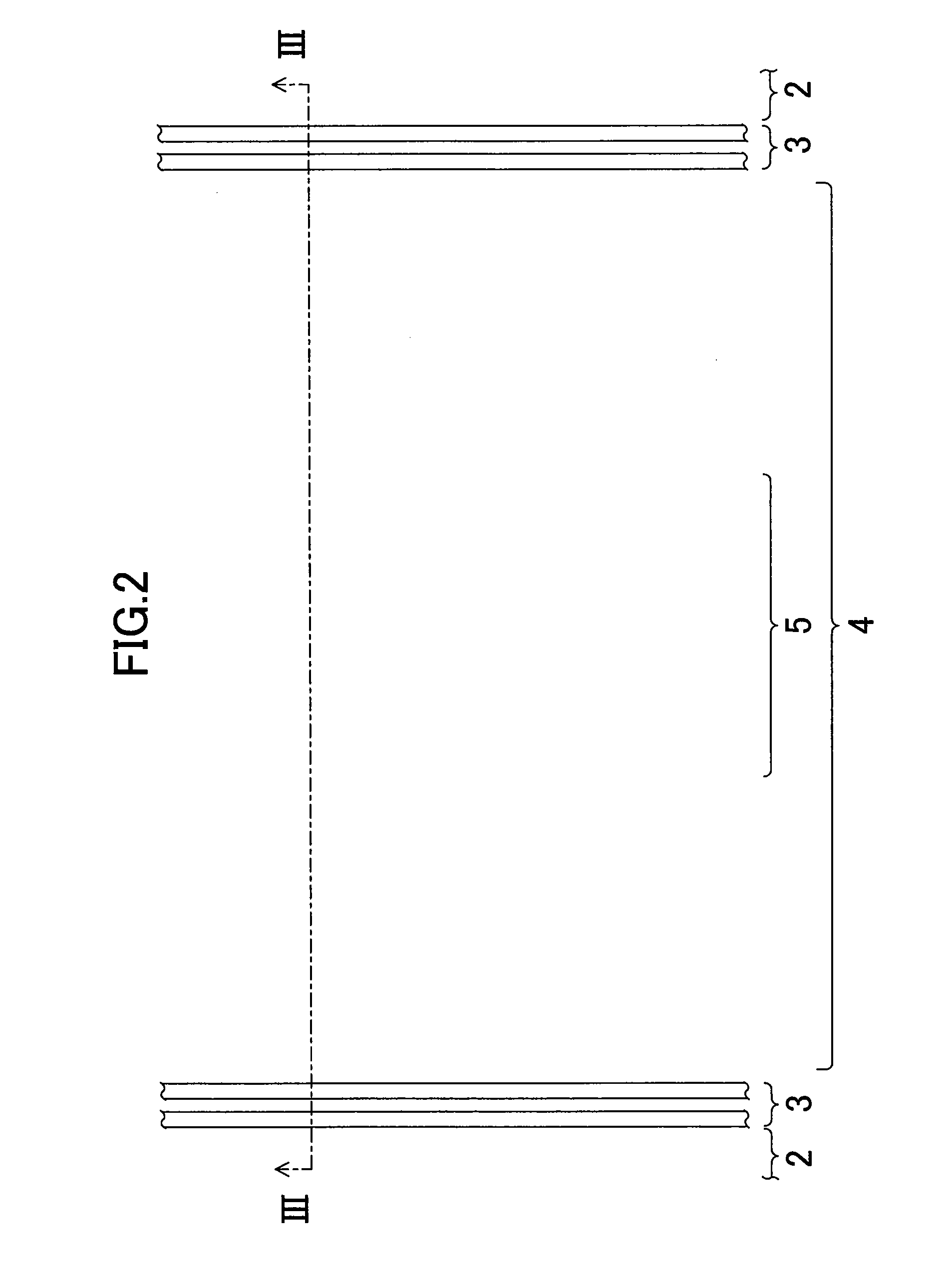
[0070]As shown in FIG. 1, in the semiconductor device of the first embodiment, a plurality of circuit regions 2 having functional elements (not shown) electrically connected by interconnects and vias connected to the interconnects are arranged at a distance from each other in a matrix pattern in a wafer-state semiconductor substrate 1. Each circuit region 2 is surrounded by an annular seal ring 3 including at least one line of line vias. A “line via” herein indicates, for example, a line-shaped via connected along a line-shaped interconnect formed in a first interlayer insulating film. Two lines of line vias are formed in the first embodiment. A scribe region 4 is formed between adjacent circuit regions, that is, around each seal ring 3, as a cutting region used in a dicing process for cutting ou...

second embodiment

[0086]A second embodiment of the invention will now be described with reference to the figures. In the embodiment and modifications described below, the same elements as those of the first embodiment are denoted with the same reference numerals and characters, and description thereof will be omitted. In the second embodiment, a dummy pattern formed by dummy interconnects or dummy vias is formed in the scribe region 4.

[0087]FIGS. 6A and 6B are partial enlarged plan views of a scribe region 4 provided between adjacent circuit regions 2. FIG. 6A shows one of a plurality of interlayer insulating films 6 which has a first dummy pattern 12 formed by an interconnect pattern. FIG. 6B shows one of the plurality of first interlayer insulating films 6 which has a second dummy pattern 13 formed by an interconnect pattern. FIG. 7 shows a cross-sectional view taken along line VII-VII in FIGS. 6A and 6B.

[0088]As shown in FIGS. 6A, 6B, and 7, the first dummy pattern 12 formed in the first interlaye...

third embodiment

[0163]A third embodiment of the invention will now be described with reference to the figures. In the third embodiment, the same elements as those of the first embodiment are denoted with the same reference numerals and characters, and description thereof will be omitted. In the third embodiment, a dummy pattern formed by dummy vias 16 is formed in a scribe region 4.

[0164]FIG. 19 shows a semiconductor device according to the third embodiment. FIG. 19 is a cross-sectional view of a scribe region 4 provided between adjacent circuit regions 2.

[0165]As shown in FIG. 19, in the semiconductor device of the third embodiment, a dummy pattern formed by a plurality of dummy vias 16 is formed in a plurality of first interlayer insulating films 6. The dummy pattern is formed so that every part of the scribe region 4, especially a blade dicing region 5, has dummy vias 16 when viewed two-dimensionally.

[0166]The dummy vias 16 are thus formed so as to cover the scribe region 4 when viewed two-dimen...


PUM


Abstract

A semiconductor device includes a semiconductor substrate, a diffusion layer conductive film formed on the semiconductor substrate, an interlayer insulating film layered on the semiconductor substrate, an interconnect pattern and a via pattern formed in the interlayer insulating film, a plurality of circuit regions formed in the semiconductor substrate, and a scribe region formed around the circuit regions and separating the circuit regions from each other. The diffusion layer conductive film is not formed at least in a region to which laser light is emitted in the scribe region.

Description

CROSS REFERENCE TO RELATED APPLICATION[0001]This application claims priority under 35 U.S.C. §119 on Patent Application No. 2007-283733 filed in Japan on Oct. 31, 2007 and Patent Application No. 2008-87906 filed in Japan on Mar. 28, 2008, the entire contents of which are hereby incorporated by reference.BACKGROUND OF THE INVENTION[0002]1. Field of the Invention[0003]The invention relates to a semiconductor device having a multilayer interconnect structure.[0004]2. Background Art[0005]In a semiconductor device having a multilayer interconnect structure, interconnect layers are generally formed by embedding a metal film in grooves formed in an interlayer insulating film of each interconnect layer (a damascene method). In the damascene method, grooves are formed in a semiconductor substrate, and a metal film is then deposited on the whole surface of the semiconductor substrate. An unnecessary metal film is removed by, e.g., a Chemical Mechanical Polishing (CMP) method so that the metal...

Claims


Application Information

Patent Timeline
Patent Type & Authority Applications(United States)
IPC IPC(8): H01L23/544
CPCH01L21/78H01L23/585H01L2924/0002H01L2924/00
Inventor TAKEMURA, KOJIKUMAKAWA, TAKAHIROMATSUSHIMA, YOSHIHIRO
Owner PANASONIC CORP
Why Eureka
Try Eureka