Die scale strain gauge

a technology of strain gauge and die, which is applied in the direction of fluid pressure measurement, fluid pressure measurement by electric/magnetic elements, instruments, etc., can solve the problems of strain damage to the chips, significant failure mode of integrated circuit chips, and gauges usually made of metal foils

Active Publication Date: 2009-05-07
SEMICON COMPONENTS IND LLC
View PDF10 Cites 5 Cited by
  • Summary
  • Abstract
  • Description
  • Claims
  • Application Information

AI Technical Summary

Benefits of technology

[0013]In an illustrative example, the strain gauge system may be operated as one or more legs in a resistance measuring bridge where the other resistances required by the bridge are off the chip. However, in other illustrative examples the other resistors may be fashioned on or in the chip.

Problems solved by technology

A significant failure mode in integrated circuit chips stems from strains generated during the fabrication of the chip and by environmental conditions including internally generated heat.
The strains may damage the chips.
These prior art strain gauges are usually made of metal foils, but are not suitable for measuring strains at the integrated circuit die level.
Others have developed Moire interferometry that can detect and measure distortion or warpage of an integrated circuit package, but such techniques cannot be use to measure the chip itself, since it is hidden within the package.
Such strain gauges are unwieldy and difficult to use on a die.
Such junctions may form complex circuitry from intrinsic electronic components (diodes, transistors, capacitors) that may adversely affect strain measurements.
Another limitation of such semiconductor strain gauges is that they cannot be easily arranged to measure vertical strain of an integrated circuit.
The known prior art present limitations where: traditional strain gauges are simply not suitable for application to integrated circuit dies or they are more complex to fabricate and use.

Method used


Image

  • Die scale strain gauge
  • Die scale strain gauge
  • Die scale strain gauge

Examples


Embodiment Construction

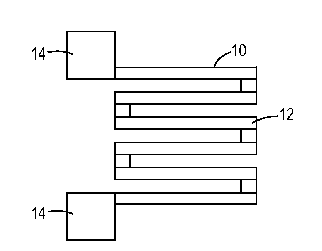
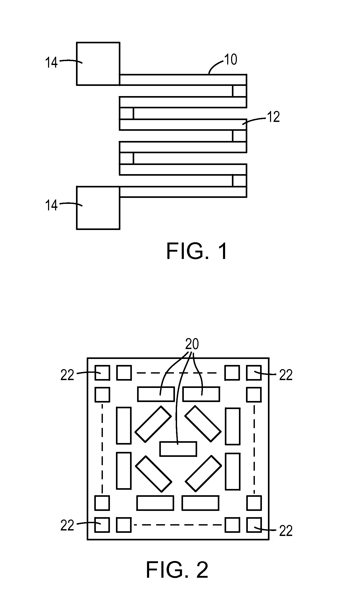
[0028]FIG. 1 is an illustrative arrangement of a serpentine pattern 10 of a deposited resistive material 12 on the surface of a chip that may be used as a strain gauge. Larger pads 14 may be used for making electrical connections. Depositing a resistive material, usually a metal, is sometimes referred to as “metallization,” is precisely controlled using current photo-lithographic deposition techniques. The width can be small and the length large to detect very small strains. As well known in the art, as the chip expands, say due to thermal conditions, the resistive element elongates. The length increases and the width decreases and the resistance of the element therefore increases. This is due to corresponding to well known relationships. As mentioned before, it is noteworthy that this embodiment uses the change in resistance of a deposited metal or metal-like material and does not use semiconductor elements created typical semiconductor processes, e.g. grown, diffused, etc. A depos...


PUM

PropertyMeasurementUnit
resistancesaaaaaaaaaa
resistanceaaaaaaaaaa
temperatureaaaaaaaaaa

Abstract

A chip with resistive, metallic strain gauges distributed on surfaces on and buried within the chip. Also, vertically arranged vias and vertical thin film resistive strain gauges are described. The resistive strain gauges can be multiplexed wherein strain can be measured across the topology of the chip in each of the top, bottom and buried layers and any vertical strain. The resistive strain gauges may be in serpentine patterns and may be arranged on via or on vertical edges of grooves that extend from an upper or lower surface of the chip to buried layers. In this fashion, the distributed strain gauges may be used to map the strain throughout the body of a chip. A Kelvin bridge may be used to measure the strain, but other such measuring techniques and devices may be used.

Description

BACKGROUND OF THE INVENTION[0001]1. Field of the Invention[0002]The present application relates to a method and apparatus for measuring and mapping strain on an integrated circuit die, and more particularly to using strain gauges that correlate resistance changes to strain at the die level.[0003]2. Background Information[0004]A significant failure mode in integrated circuit chips stems from strains generated during the fabrication of the chip and by environmental conditions including internally generated heat. The strains may damage the chips. Measuring strain at the chip level during chip fabrication may suggest changes to the chip fabrication processes to reduce the strain and improve the production yield.[0005]Use of strain gauges is well known in the art for measuring strains on surfaces. They are used by fixing or bonding the strain gauge to the article, and using the strain gauge as one or more legs in a Wheatstone Bridge or equivalent circuit. As stresses on the article cause...

Claims


Application Information

Patent Timeline
Patent Type & Authority Applications(United States)
IPC IPC(8): G01L9/04
CPCG01L1/2262G01L1/2287G01L1/2281
Inventor IRVING, SCOTTLIU, YONGLUK, TIMWAH
Owner SEMICON COMPONENTS IND LLC
Why Eureka
Try Eureka