
Substrate processing apparatus

Pending Publication Date: 2009-05-07
NTT MOBILE COMM NETWORK INC
View PDF2 Cites 17 Cited by
  • Summary
  • Abstract
  • Description
  • Claims
  • Application Information

AI Technical Summary

Benefits of technology

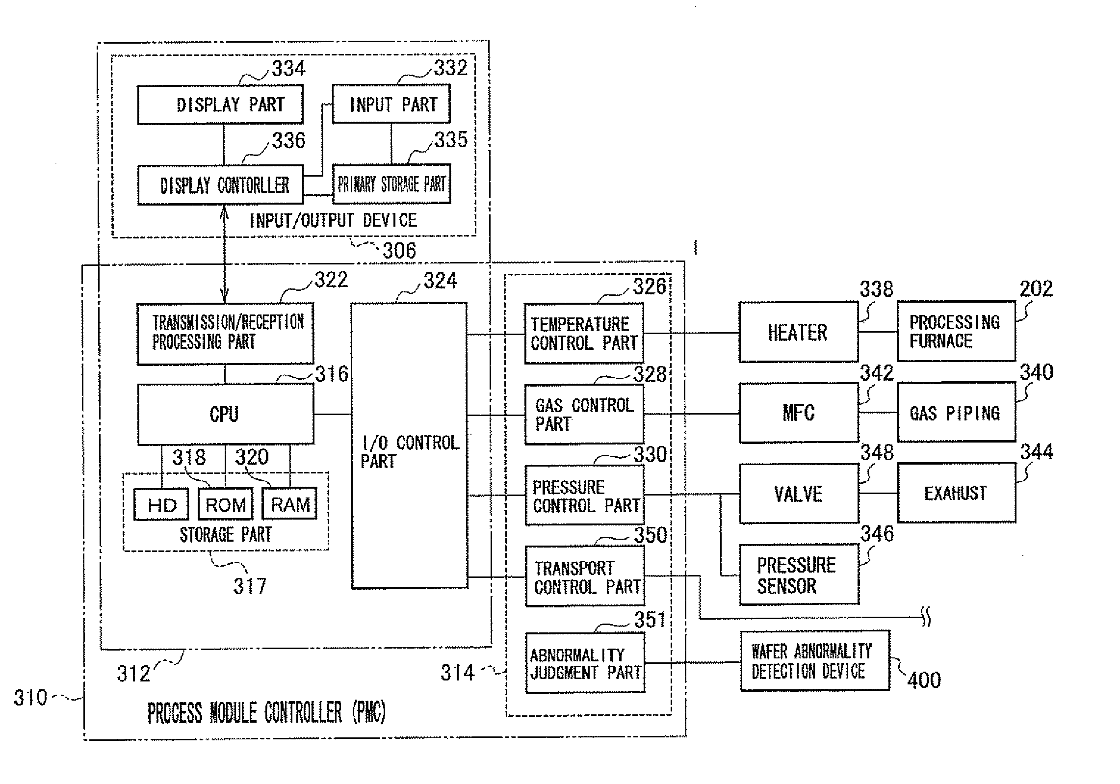
[0012]According to the present invention, the transfer state of the wafer held on the substrate holding tool and the detail-information thereof can be displayed on the same screen. This makes it possible to confirm the transfer state of the wafer and the detail-information of the wafer. In addition, the designation of error processing at the time of the occurrence of abnormality can be performed on the same screen. Therefore, stop of the processing does not occur, by a slight error (simple detection error). Also, error cancellation can be confirmed instantaneously with completion of the error recovery processing, thus improving operation efficiency as a result.

Problems solved by technology

Therefore, stop of the processing does not occur, by a slight error (simple detection error).

Method used


Image

  • Substrate processing apparatus
  • Substrate processing apparatus
  • Substrate processing apparatus

Examples


Embodiment Construction

[0024]In a best mode for carrying out the invention, a vertical substrate processing apparatus (simply called a processing apparatus hereafter) for performing oxidization / diffusion processing and CVD processing to a substrate is selected as a substrate processing apparatus, which is, for example, used as a processing apparatus in a manufacturing method of a semiconductor device (IC).

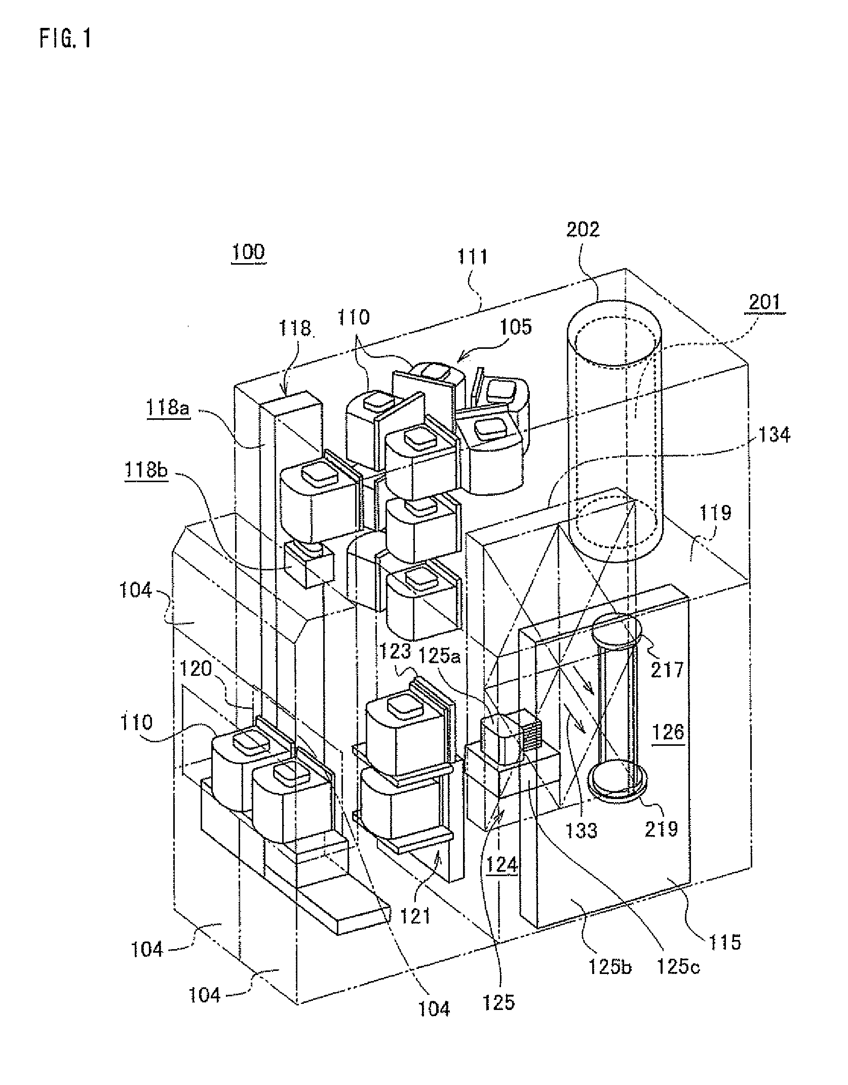
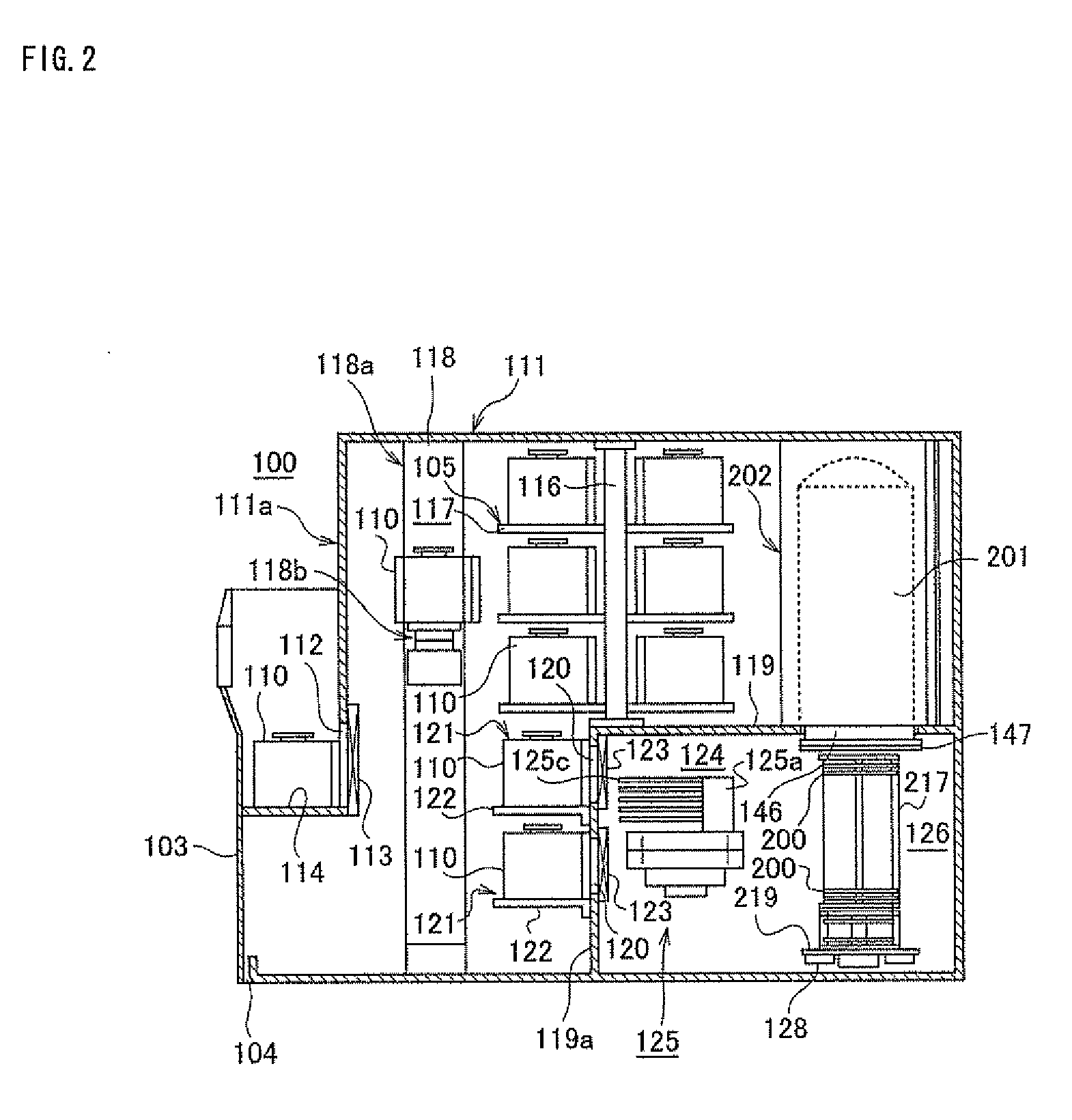
[0025]First, explanation will be given for the substrate processing apparatus according to an embodiment of the present invention, with reference to FIG. 1 and FIG. 2.

[0026]FIG. 1 is shown as a perspective of the substrate processing apparatus applied to the present invention. Also, FIG. 2 is a side perspective of the substrate processing apparatus shown in FIG. 1.

[0027]As shown in FIG. 1 and FIG. 2, FOUP (Front Opening United Pod. Called as pods hereafter) 110, being wafer carriers, are used in a substrate processing apparatus 100. A front maintenance port 103 is opened in front of a front side wall 111...


PUM


Abstract

To simultaneously display a transfer state of substrates (wafers) held on a substrate holding tool and detail-information thereof on the same screen. In a substrate processing apparatus that loads a substrate holding tool, on which a plurality of substrates are placed, into a furnace, and applies prescribed processing thereto, a whole body of boats, as a boat image view of transfer information regarding the substrates on the substrate holding tool, is displayed in an operation screen, and detail-information of a substrate of each area is displayed in the operation screen, with the whole body of the boats divided into a plurality of areas.

Description

BACKGROUND[0001]1. Technical Field[0002]The present invention relates to a substrate processing apparatus, and particularly relates to the substrate processing apparatus for displaying on a screen a substrate stacking state of a substrate holding tool provided in the substrate processing apparatus.[0003]2. Description of Related Art[0004]Conventionally, in a method of displaying a transfer state of a wafer to a boat, an image of a boat is displayed on a screen, and by classifying wafers by color in a figure of a boat image, the kinds of the wafers on the boat is clarified.[0005]For example, patent document 1 discloses a technique of classifying each wafer on the wafer boat by color according to their kinds, based on slot information of the boat.(Patent Document 1)Japanese Patent Laid Open No. 11-121586[0006]Conventionally, when processing of deleting the wafer actually having abnormality is performed, for example, it is necessary to switch a screen from the screen of displaying a tr...

Claims


Application Information

Patent Timeline
IPC IPC(8): B05C11/00
CPCH01L21/67253H01L21/67288H01L21/67276
Inventor YONEDA, AKIHIKOFUJIMOTO, KENICHI
Owner NTT MOBILE COMM NETWORK INC
Learn More