Panel structure and manufacturing method thereof

a manufacturing method and panel technology, applied in the direction of semiconductor devices, electrical apparatus, transistors, etc., can solve the problems of poor process stability of the ltps process, poor display panel aperture ratio, and reduced light utilization of the display panel. achieve the effect of high electron mobility

Inactive Publication Date: 2009-05-07
WINTEK CORP
View PDF4 Cites 104 Cited by
  • Summary
  • Abstract
  • Description
  • Claims
  • Application Information

AI Technical Summary

Benefits of technology

[0009]The invention is directed to a display panel and a manufacturing method thereof. ZnO is used to be one of the materials of transistors of at least one of a control circuit and a display circuit, so that the transistors have high electron mobility and the manufacturing process of the transistors is compatible with that of a-Si material TFTs.

Problems solved by technology

However, the increase of the area of the storage capacitor reduces the aperture ratio of the display panel, so that the light utilization of the display panel decreases accordingly.
In addition, the process stability of the LTPS process is poorer and the cost of manufacturing equipment is higher.
Moreover, the excimer laser technology is used to convert a a-Si material into a LTPS material to obtain the LTPS material TFT, so that the LTPS material TFT is usually lack of the uniformity after the process.
Thus, the display quality of the display panel is reduced.

Method used


Image

  • Panel structure and manufacturing method thereof
  • Panel structure and manufacturing method thereof
  • Panel structure and manufacturing method thereof

Examples


first embodiment

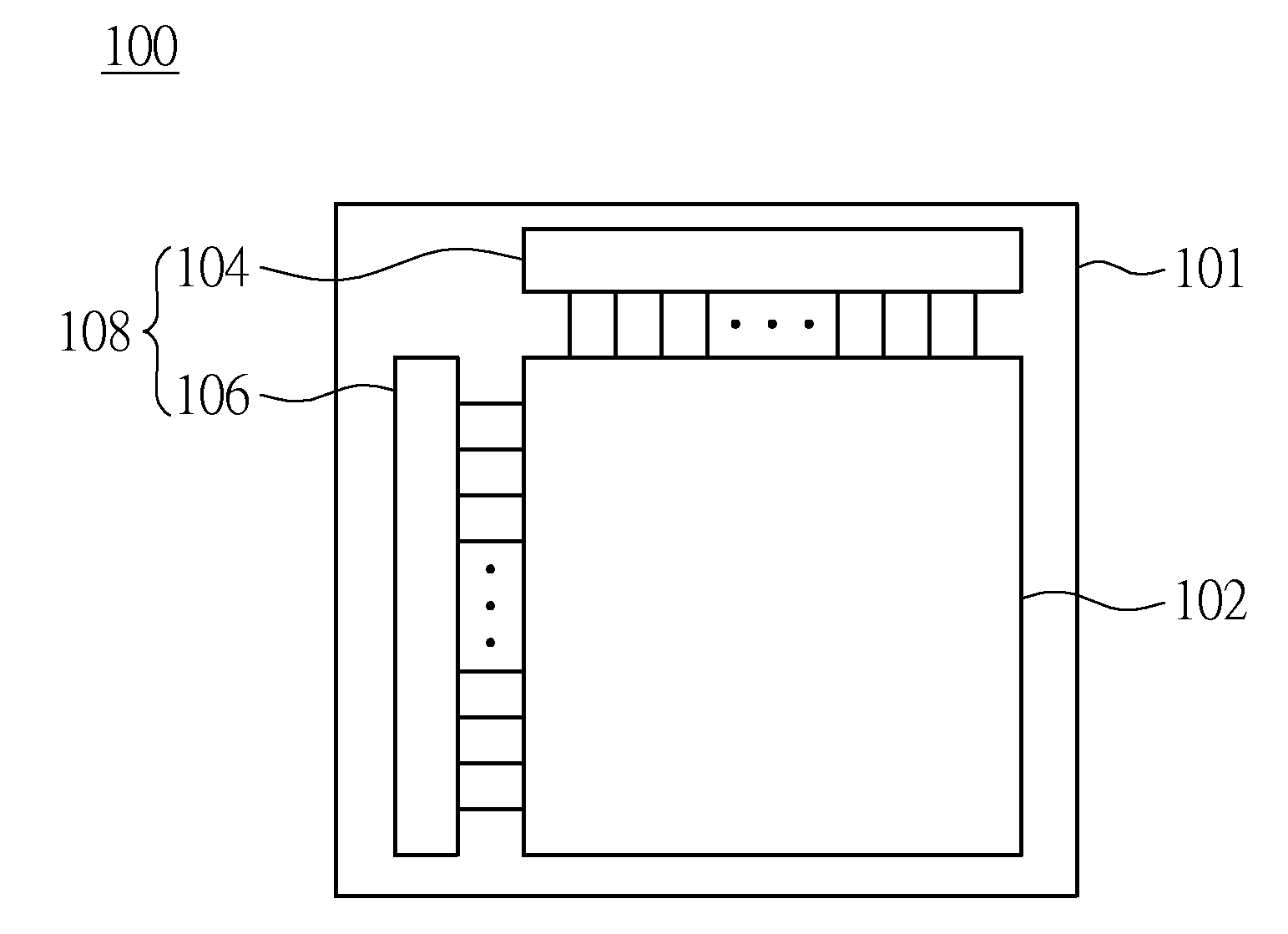
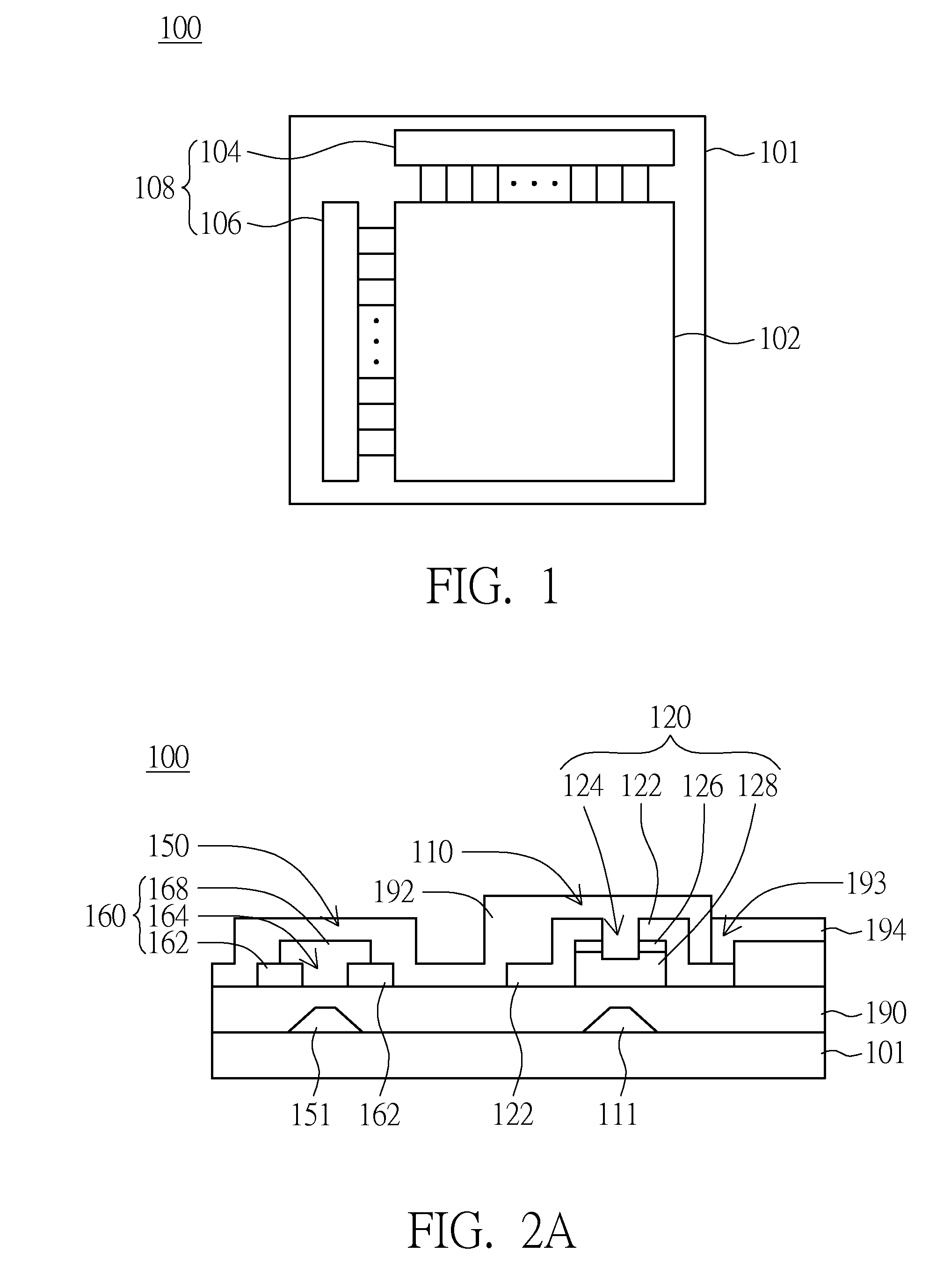
[0033]Referring to FIG. 1 and FIG. 2A at the same time, FIG. 1 illustrates a panel structure according to a first embodiment of the invention, and FIG. 2A is a cross-sectional view of the panel structure in FIG. 1. The panel structure 100 has a substrate 101, several first transistors 110 and second transistors 150. Only one first transistor 110 and one second transistor 150 are shown in FIG. 2A to simplify the figure.

[0034]The substrate 101 has a display circuit 102 and a control circuit 108. The display circuit 102 is driven by the control circuit 108 to display frames. The first transistor 110 is disposed at the display circuit 102 of the substrate 101, and the first transistor 110 has a first active layer 128. The second transistor 150 is disposed at the control circuit 108 of the substrate 101, and the second transistor 150 has a second active layer 168. The materials of at least one of the first active layer 128 and the second active layer 168 include ZnO. Therefore, at least ...

second embodiment

[0060]Referring to FIG. 7A, a cross-sectional view of a panel structure according to a second embodiment of the invention is illustrated. A second island structure 260 of the panel structure 200 in FIG. 7A and the second island structure 160 of the panel structure 100 in FIG. 2A are different. Although the second island structure 260 of the panel structure 200 has a second electrode layer 262, a second opening 264 and a second active layer 268 as well, the second active layer 268 is disposed on an insulation layer 290. The second electrode layer 262 is disposed above the second active layer 268, and the second opening 264 penetrates the second electrode layer 262 to expose the second active layer 268.

[0061]In order to simplify the figure, only one first transistor 210 and one second transistor 250 are illustrated in FIG. 7A. However, as stated early, the panel structure 200 differs from the panel structure 100 (as shown in FIG. 2A) only in the second island structure 260. Thus, the ...

third embodiment

[0072]Referring to FIG. 10A, a cross-sectional view of a panel structure according to a third embodiment of the invention is illustrated. A second transistor 350 of the panel structure 300 in FIG. 10A differs from the second transistor 150 of the panel structure 100 in FIG. 2A. Although the second transistor 350 has a second gate 351 and a second island structure 360 as well, the second gate 351 is disposed on an insulation layer 390 and the second island structure 360 is disposed between the insulation layer 390 and a substrate 301.

[0073]The second island structure 360 similarly has a second electrode layer 362, a second opening 364 and a second active layer 368. The second electrode layer 362 is disposed on the substrate 301. The second opening 364 penetrates the second electrode layer 362 to expose the substrate 301. The second active layer 368 covers the second opening 364.

[0074]In the embodiment, the panel structure 300 includes several first transistors 310, second transistors...


PUM


Abstract

A panel structure and a manufacturing method thereof are provided. The panel structure is disposed in a display device. The panel structure includes a substrate, several first transistors and second transistors. The substrate has a display circuit and a control circuit. The first transistors are disposed at the display circuit of the substrate. Each of the first transistors has a first active layer. The second transistors are disposed at the control circuit of the substrate. Each of the second transistors has a second active layer. The materials of at least one of the first active layer and the second active layer include ZnO.

Description

[0001]This application claims the benefit of Taiwan application Serial No. 096141932, filed Nov. 6, 2007, the subject matter of which is incorporated herein by reference.BACKGROUND OF THE INVENTION[0002]1. Field of the Invention[0003]The invention relates in general to a panel structure and a manufacturing method thereof, and more particularly to a panel structure having a control circuit and a display circuit on a substrate and a manufacturing method thereof.[0004]2. Description of the Related Art[0005]Following the development of the technology, a display panel having a control circuit and a display circuit on the same substrate has been gradually emphasized. Each of the display circuit and the control circuit is driven by several thin film transistors (called TFT in the following). The same semi-conducting material is usually adopted to be the materials of the TFTs of the display circuit and the control circuit, such as an amorphous silicon (a-Si) material or a low temperature po...

Claims


Application Information

Patent Timeline
Patent Type & Authority Applications(United States)
IPC IPC(8): H01L27/088H01L21/8232
CPCH01L27/1225H01L29/7869H01L27/1251
Inventor WANG, WEN-CHUNKANG, HEN-TACHU, CHIEN-TZU
Owner WINTEK CORP
Why Eureka
Try Eureka