

Delay locked loop and operating method thereof
a delay lock and loop technology, applied in the field of semiconductor design technology, can solve problems such as system malfunction, problem of conventional dll, and inability to obtain internal clocks, and achieve the effect of stable operation
- Summary
- Abstract
- Description
- Claims
- Application Information
AI Technical Summary
Benefits of technology
Problems solved by technology
Method used
Image

Examples
Embodiment Construction
[0069]Hereinafter, a delay locked loop (DLL) and an operating method thereof in accordance with the invention will be described in detail with reference to the accompanying drawings.
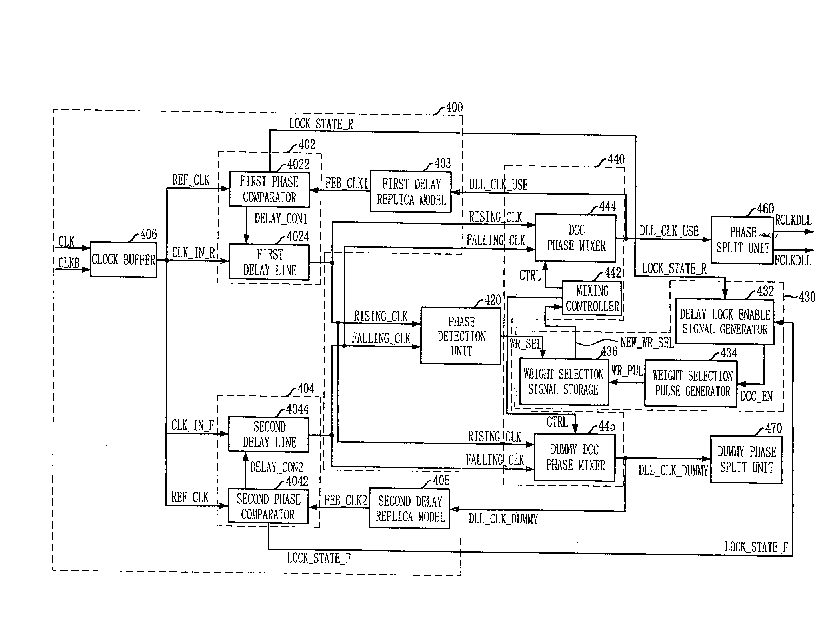
[0070]FIG. 4 is a block diagram of a DLL in accordance with an embodiment of the invention.
[0071]Referring to FIG. 4, the DLL in accordance with the embodiment of the invention includes a delay-locking unit 400, a phase detection unit 420, a weight storage unit 430 and a phase mixing unit 440. The delay-locking unit 400 generates a first delay clock RISING_CLK corresponding to a first clock edge, e.g., rising edge, of a reference clock REF_CLK, and a second delay clock FALLING_CLK corresponding to a second clock edge, e.g., falling edge, of the reference clock REF_CLK for achieving a delay-locking. The phase detection unit 420 detects a phase difference between the first and second delay clocks RISING_CLK and FALLING_CLK to output a weight selection signal WR_SEL. The weight storage unit 430 stores the w...
PUM
 Abstract
Description
Claims
Application Information