Package structure of a light emitting diode device and method of fabricating the same

a technology of light emitting diodes and packaging structures, which is applied in the manufacture of semiconductor/solid-state devices, semiconductor devices, electrical devices, etc., can solve the problems of reducing the use ratio of back light modules

Inactive Publication Date: 2009-05-14
ADVANCED OPTOELECTRONICS TECH
View PDF1 Cites 33 Cited by
  • Summary
  • Abstract
  • Description
  • Claims
  • Application Information

AI Technical Summary

Benefits of technology

[0012]An aspect of the present invention is to provide a package structure for light emitting diode devices and a method of fabricating the same. A dual brightness enhancement film is used for the light emitting diode devices to enhance the intensity of a light with a specific polarization orientation. With enhanced intensity, the usage ratio of the light in the back light module of an LCD and the image quality produced by the LCD can be increased.

Problems solved by technology

(1) Side-emitting type structure: a light source is placed on the side of a module and a light guide plate is manufactured by molding injection without printed patterns. This structure is usually used for back light modules smaller than 18 inches in size. The features of this type include lightweight, a thin profile, narrow frame, and low power consumption. At present, some large size back light modules adopt this kind of structure.
(2) Direct type structure: For super-large size back light modules, side-emitting type structures exhibit comparatively poor features of weight, power consumption, and brightness. A direct type structure with light sources at the bottom but without a light guide plate is developed. Light from a lamp or an LED will be reflected by a reflector and evenly diffused by a diffuser. The light then passes through the front surface of the LCD panel. Because of larger space, more lamps can be used in accordance with larger panels. This type has the advantages of better color, wide viewing angle, and a simpler structure. It is suitable for LCD and liquid crystal TV applications. However, the thickness, weight and power consumption are increased. Moreover, high power consumption (when using a cold cathode fluorescent lamp), uneven brightness, and overheating are problems that need to be solved.
However, there is no dual brightness enhancement film in the package structure of the device.

Method used


Image

  • Package structure of a light emitting diode device and method of fabricating the same
  • Package structure of a light emitting diode device and method of fabricating the same
  • Package structure of a light emitting diode device and method of fabricating the same

Examples


Embodiment Construction

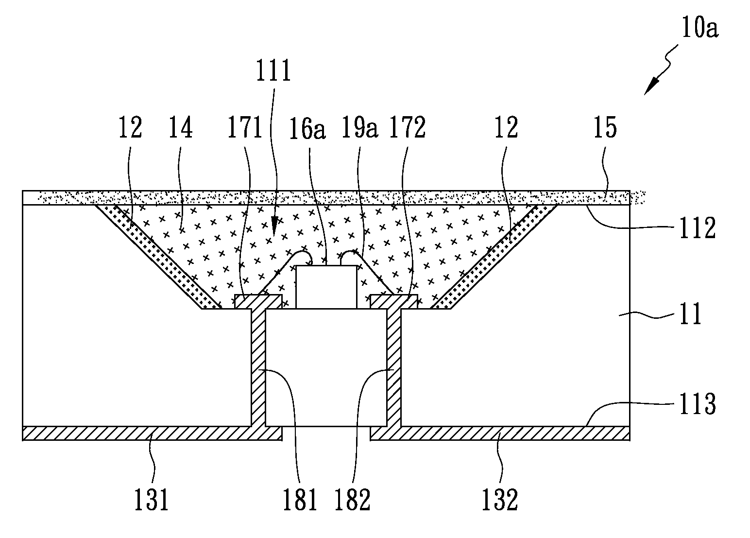
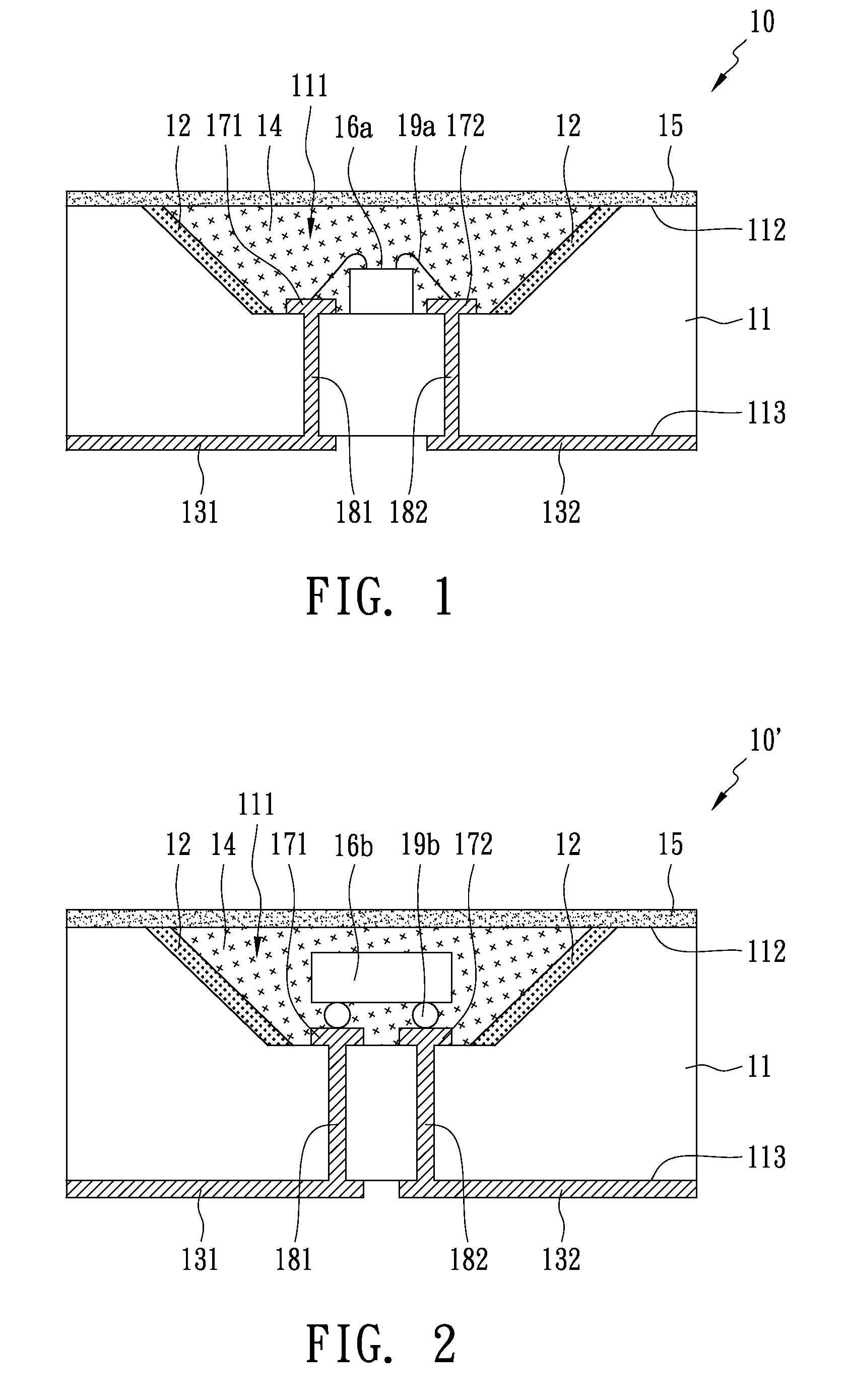
[0029]FIG. 1 is a cross-sectional diagram showing a light emitting diode device in accordance with the present invention. A light emitting diode device 10 comprises a substrate 11 having a reflective cavity 111, a die 16a mounted inside the reflective cavity 111, a reflective layer 12 disposed on the surface of the reflective cavity 111, a plurality of electrodes 131-132 disposed under the surface of the substrate 11 which is opposite to the reflective cavity 111, and a dual brightness enhancement film 15 overlaid on the reflective cavity 111. A concave reflective cavity 111 is formed on the first surface 112 of the substrate 11 and the electrodes 131-132 are disposed under the second surface 113 of the substrate 11. The material of the substrate 11 can be a silicon material, a ceramic material, a polymeric material, a glass, or a low temperature co-fired ceramic material. A plurality of solder pads 171-172 are disposed on the bottom of the reflective cavity with a cup shape and the...


PUM


Abstract

A package structure for light emitting diode devices comprises a substrate having a reflective cavity, a die mounted inside the reflective cavity, a reflective layer disposed on the surface of the reflective cavity, a plurality of electrodes disposed under the surface of the substrate which is opposite to the reflective cavity, and a dual brightness enhancement film overlaid on the reflective cavity. The dual brightness enhancement film efficiently reflects the polarized light that is generated from the die and is not in a transparent direction back to the reflective layer. Subsequently, this light is reflected from the reflective layer to the dual brightness enhancement film. The portions of the reflected light propagating in the same direction as the transparent direction will transmit through the package structure.

Description

BACKGROUND OF THE INVENTION[0001]1. Field of the Invention[0002]The present invention relates to a package structure for light emitting diode (LED) devices and a method of fabricating the same, and more particularly to an LED device with the ability to increase the intensity of a specific polarized light.[0003]2. Description of the Related Art[0004]LEDs (light emitting diode) have advantages including compact size, high illuminating efficiency and long life. They are anticipated to be the best light source for the future. Because of the rapid development of LCDs (liquid crystal display) and the trend of full-sized screen displays, white light LEDs are applied not only to indication lamps and large size screens but also to consumer electronics products (e.g., cell phones and personal digital assistants).[0005]With breakthroughs in the research of new materials, illuminating efficiency and output power of LEDs are increased continuously and the brightness of LEDs are gradually approac...

Claims


Application Information

Patent Timeline
Patent Type & Authority Applications(United States)
IPC IPC(8): H01L33/00H01L21/02H01L33/44H01L33/48
CPCH01L33/44H01L33/486H01L2224/48091H01L2224/48227H01L2924/00014
Inventor TSENG, WEN LIANGCHEN, LUNG HSIN
Owner ADVANCED OPTOELECTRONICS TECH
Why Eureka
Try Eureka