Shift register circuit

Active Publication Date: 2009-05-14
TRIVALE TECH
View PDF4 Cites 73 Cited by
  • Summary
  • Abstract
  • Description
  • Claims
  • Application Information

AI Technical Summary

Benefits of technology

[0022]It is an object of the present invention to provide a bidirectional shift register i

Problems solved by technology

However, when the operation of the gate line drive circuit is switched to the backward shift (backward scanning) after that, the followin

Method used


Image

  • Shift register circuit
  • Shift register circuit
  • Shift register circuit

Examples


embodiment 1

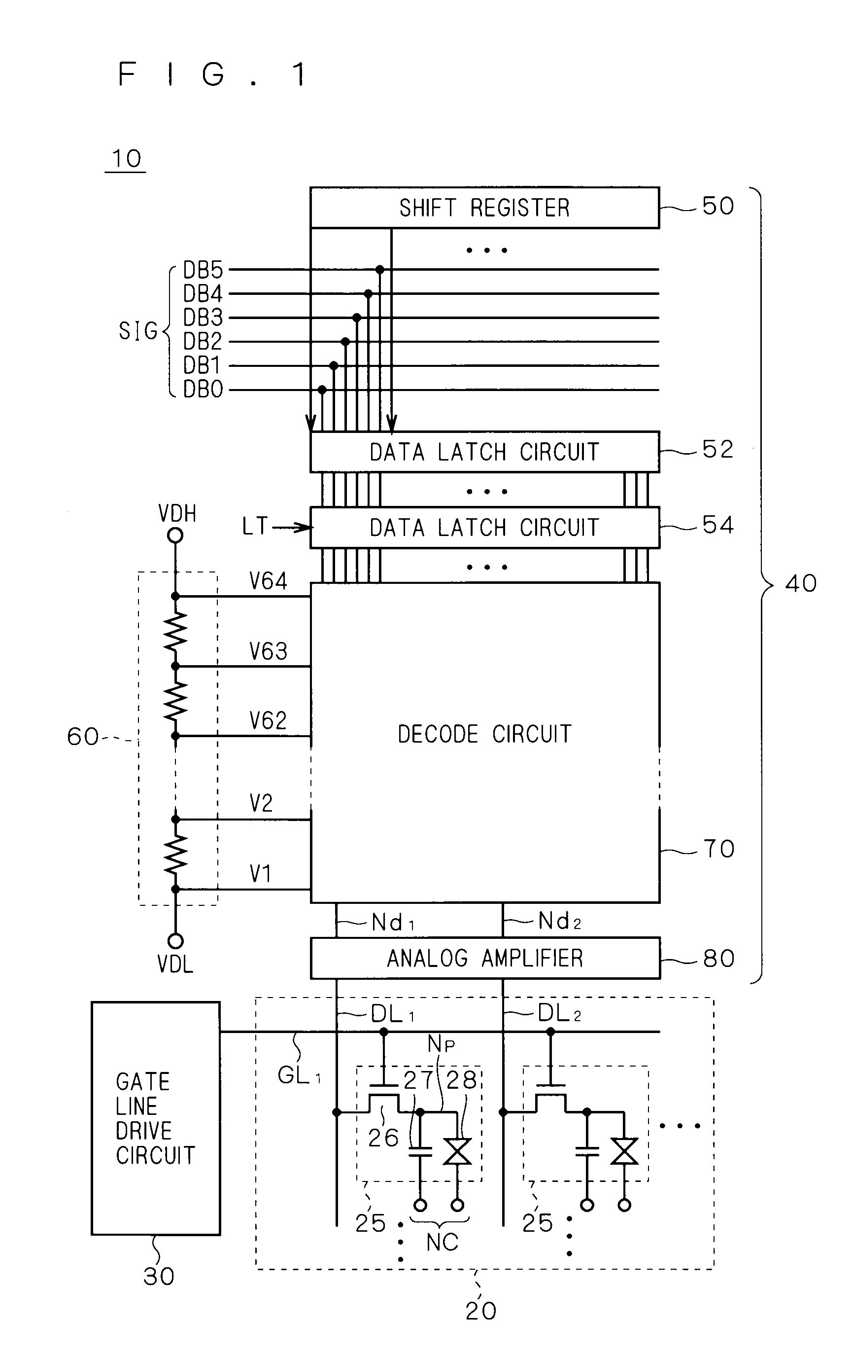
[0060]FIG. 1 is a schematic block diagram showing a constitution of a display device according to an embodiment 1 of the present invention in which an entire constitution of a liquid crystal display device 10 is shown as a representative example of a display device.

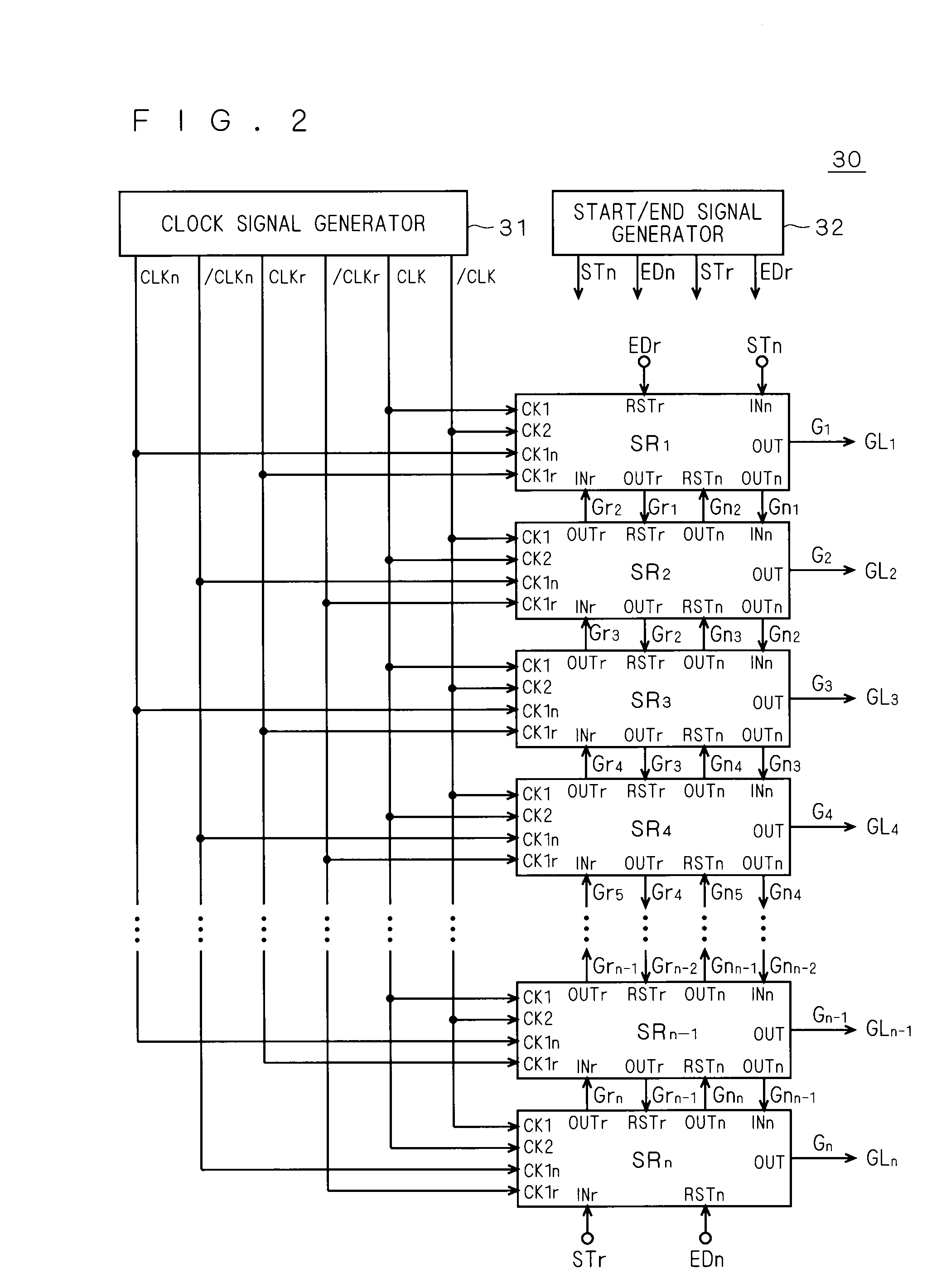
[0061]The liquid crystal display device 10 includes a liquid crystal array unit 20, a gate line drive circuit (scanning line drive circuit) 30, and source driver 40. Although it will be clear from a description below, a bidirectional shift register according to this embodiment of the present invention is mounted on the gate line drive circuit 30.

[0062]The liquid crystal array unit 20 includes a plurality of pixels 25 arranged in the form of a matrix. Gate lines GL1, GL2, . . . (generic term “gate line GL”) are arranged in rows of pixels (referred to also as “pixel line”), and data lines DL1, DL2, . . . (generic term “data line DL”) are arranged in columns of pixels (referred to also as “pixel column). In FIG. 1, pixels 25...

embodiment 2

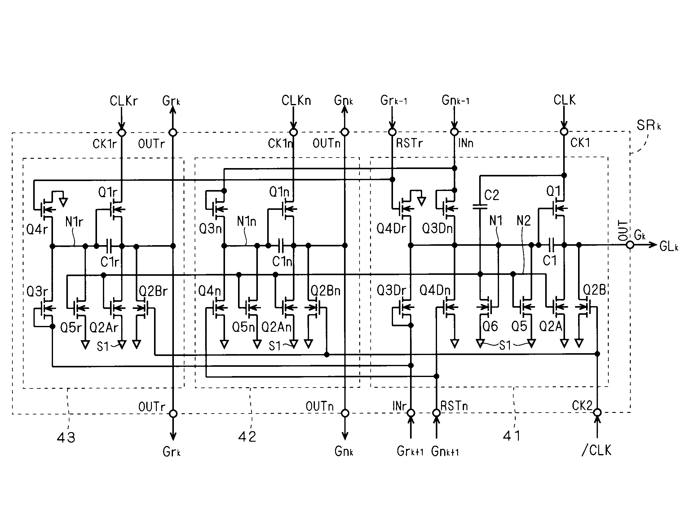
[0174]FIG. 12 is a circuit diagram of the unit shift register SR according to an embodiment 2. Similar to the embodiment 1, since the unit shift registers SR1 to SRn are the same circuits basically, a k-stage unit shift register SRk is shown also here representatively.

[0175]The unit shift register SR according to this embodiment is provided with a second forward clock terminal CK2n and a second backward clock terminal CK2r. Although the second forward clock terminal CK2n receives the forward clock CLKn or / CLKn similar to the first forward clock terminal CK1n, it receives the one opposite to that supplied to the first forward clock terminal CK1n. As shown in FIG. 12, for example, in the unit shift register SRk, in which the forward clock CLKn is supplied to the first forward clock terminal CK1n, the forward clock / CLKn is supplied to the second forward clock terminal CK2n.

[0176]Although the second backward clock terminal CK2r receives the backward clock CLKr or / CLKr similar to the...

embodiment 3

[0181]FIG. 13 is a circuit diagram showing the unit shift register SR according to an embodiment 3. Also in this drawing, the k-stage unit shift register SRk is representatively shown.

[0182]According to the unit shift register SRk in FIG. 7, when the clock signal CLK becomes L level during the unselected period, the transistors Q5, Q5n, and Q5r are turned off and the nodes N1, N1n, and N1r become L level of high impedance. Thus, during that period, the levels of the nodes N1, N1n, and N1r are likely to be affected by a noise and the like. Thus, according to this embodiment, the measures against the problem are proposed.

[0183]According to the unit shift register SR in this embodiment, the forward clock CLKn or / CLK that is opposite to the one inputted to the first forward clock terminal CK1n is inputted to the forward reset terminal RSTn, and the backward clock CLKr or / CLKr that is opposite to the one inputted to the first backward clock terminal CK1r is inputted to the backward res...


PUM


Abstract

A bidirectional shift register in which an operation margin is not lowered when a shift direction of a signal is switched is provided. A unit shift register SRk at one stage of a plurality of stages of shift registers includes a gate line drive unit, a forward shift unit, and backward shift unit each capable of operating as one-stage shift register. The gate line drive unit outputs a gate line drive signal Gk to a gate line GLk in response to a previous-stage forward signal Gnk−1 and a subsequent-stage backward signal Grk+1. The forward shift unit performs only forward shift to output a forward signal Gnk to the subsequent-stage in response to the previous-stage forward signal Gnk−1, and the backward shift unit performs only backward shift to output a backward signal Grk to the previous-stage in response to the subsequent-stage backward signal Grk+1.

Description

BACKGROUND OF THE INVENTION[0001]1. Field of the Invention[0002]The present invention relates to shift register circuit only composed of same conductivity type field-effect transistors used in a scanning line drive circuit of an image display device, for example, and more particularly to a bidirectional shift register capable of inverting a shift direction of a signal.[0003]2. Description of the Related Art[0004]According to an image display device such as a liquid crystal display device (referred to as “display device” hereinafter), a gate line (scanning line) is provided for each pixel row (pixel line) of a display panel in which a plurality of pixels are arranged in the form of a matrix, and a display image is updated by sequentially selecting and driving the gate line based on one horizontal period of a display signal. As a gate line drive circuit (scanning line drive circuit) to sequentially select and drive the pixel line, that is, the gate line, a shift register performing a ...

Claims


Application Information

Patent Timeline
IPC IPC(8): G11C19/28
CPCG11C19/28G11C19/184
Inventor TOBITA, YOUICHI
Owner TRIVALE TECH
Why Eureka
Try Eureka