Pixel Sensing Circuit with Common Mode Cancellation

a sensing circuit and common mode technology, applied in the field of biometric data, can solve the problems of affecting not only the undesired, the output dynamics of the sensing circuit are not used efficiently, and the difficulty in accurately determining data in that output, etc., to achieve the effect of improving the signal-to-noise ratio (snr) of the pixel circuit and low-power pixel circuit implementation

Active Publication Date: 2009-05-14
APPLE INC
View PDF62 Cites 45 Cited by
  • Summary
  • Abstract
  • Description
  • Claims
  • Application Information

AI Technical Summary

Benefits of technology

[0012]The output of the present invention is an electronic signal that indicates the fine surface features of the detected object (e.g., an image of a fingerprint pattern). Using a charge subtraction technique at the input of the circuit integrator, the so called “common mode” signal is subtracted from the circuit output. The result is an output signal that is (a) linear, (b) free from any amplification effect due to the presence of the detected object (e.g., a finger), and (c) indicative of the detected object's fine surface geometry (e.g., indicative of the fingerprint's ridges and valleys). With the common mode signal effectively removed from the output, the circuit makes better use of the available output dynamics of the sensing pixel circuit compared to the prior art. This can improve the signal-to-noise ratio (SNR) of the pixel circuit, as well as enable low power pixel circuit implementations.

Problems solved by technology

As the ratio of data (signal) to noise decreases in an output, the difficulty in accurately determining data in that output increases.
However, adjusting the gain and offset affect not only the undesired “common mode” signal, but also the desired data (signal).
Thus in the prior art, the output dynamics of the sensing circuit are not used efficiently to reflect the presence of surface modulations, i.e., the fingerprint features.
That is, the actual voltage representing the data decreases to a point that it is difficult to detect, especially as compared to the voltage representing the common mode.
Thus, as dynamic range is compressed, the noise portion of the pixel output dominates the data, and generation of a biometric image (e.g., fingerprint) becomes more difficult and less accurate (if possible at all).

Method used


Image

  • Pixel Sensing Circuit with Common Mode Cancellation
  • Pixel Sensing Circuit with Common Mode Cancellation
  • Pixel Sensing Circuit with Common Mode Cancellation

Examples


Embodiment Construction

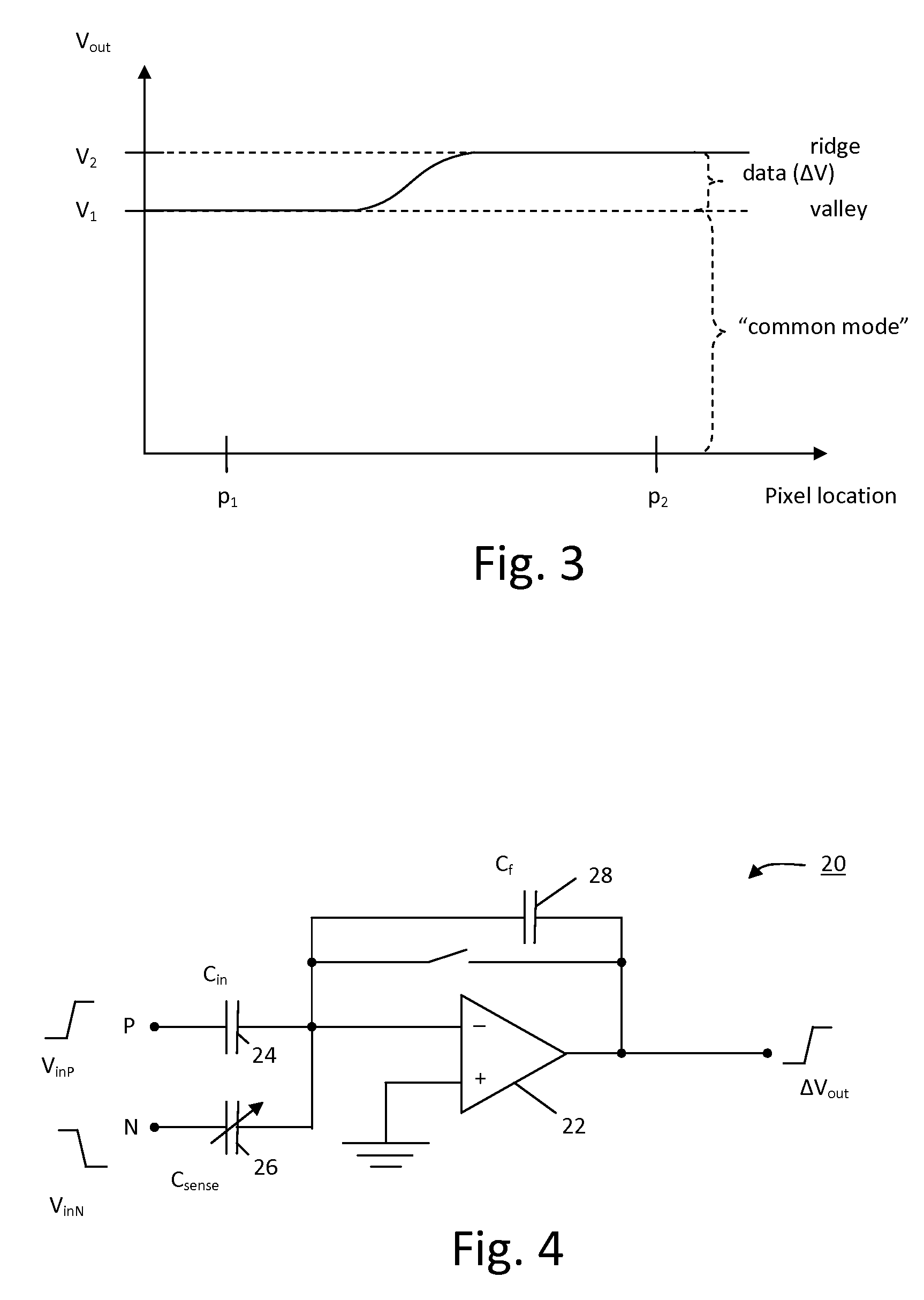
[0022]In order to remove the common mode, we have developed an improved pixel circuit 20, as illustrated in FIG. 4. Pixel circuit 20 comprises an operational amplifier 22 having an input connected to a first capacitor 24, a second capacitor 26 which serves as the sensing capacitor, and a third capacitor 26, which is the feedback capacitance (Cf). A charge P is applied to capacitor 24 as VinP, and a charge N is applied to capacitor 26 as VinN. The magnitudes of charges P and N may be different, but they are essentially of opposite phase with respect to one another.

[0023]Again, in terms of CS0, the sensing capacitance Csense, is given by

Csense={CS0intheabsenceofafingerprintridge(CS0=Csense)CS0(1-α)inthepresenceofafingerprintridge(thepixellocationptyp.approx.0.1)

In the absence of a fingerprint we obtain

Δvout=-ΔvinP·CinCf+ΔVinN·CS0Cf(2)

And in the presence of a fingerprint we obtain

Δvout=-ΔvinP·CinCf+ΔVinN·CS0Cf(1-α)or(3)Δvout=-ΔvinP·CinCf+ΔVinN·CS0Cf-ΔVinN·CS0αCf(4)

[0024]Now, we choose ...


PUM


Abstract

An improved biometric data sensing circuit, for example adapted for fingerprint sensing, uses a charge subtraction technique at the input of the circuit integrator to cancel the so called “common mode” signal from the circuit output. The result is an output signal that is (a) linear, (b) free from any amplification effect due to the presence of the detected object (e.g. a finger), and (c) indicative of the detected object's fine surface geometry (i.e., indicative of the fingerprint's ridges and valleys).

Description

CROSS-REFERENCE TO RELATED APPLICATIONS[0001]The present disclosure is related to and claims priority from copending U.S. Provisional Patent Application, Ser. No. 60 / 987,739, filed on Nov. 13, 2007, and further which, in its entirety, is hereby incorporated herein by reference.BACKGROUND OF THE INVENTION[0002]1. Field of the Invention[0003]The present invention relates to biometric data (e.g., fingerprint) sensing circuitry, and more particularly to a circuit and method for improving dynamic range in such circuitry.[0004]2. Description of the Prior Art[0005]Capacitive biometric data sensing circuits (also referred to as pixels) are well known. Such a circuit is shown and described in U.S. Pat. No. 6,512,381, incorporated herein by reference. More specifically, with reference to FIG. 1 hereof, there is shown a schematic illustration of a circuit for 10 biometric data sensing. FIG. 2 is an illustration of a device 20 implementing the circuit 10 of FIG. 1.[0006]A common application of ...

Claims


Application Information

Patent Timeline
Patent Type & Authority Applications(United States)
IPC IPC(8): G06K9/00
CPCG06K9/0002G06V40/1306
Inventor GOZZINI, GIOVANNI
Owner APPLE INC
Why Eureka
Try Eureka