Optical-waveguide sensor chip, method of manufacturing the same, method of measuring substance, substance-measuring kit and optical-waveguide sensor

a technology of optical waveguide and sensor chip, which is applied in the direction of instruments, optical elements, coatings, etc., can solve the problems of complicated procedure described and difficulty in monitoring change over time in the same sampl

Inactive Publication Date: 2009-05-14
KK TOSHIBA
View PDF3 Cites 18 Cited by
  • Summary
  • Abstract
  • Description
  • Claims
  • Application Information

AI Technical Summary

Problems solved by technology

These immunological assays are thus carried out in complicated procedure demanding addition and discharge of these reagents while weighed by the operator.
However, conventional immunological assays demand almost one hour for reaction between the primary antibody and the analyte sample and also for reaction between the analyte sample and the secondary antibody, leading to the complicated procedure described above.
As a result, it is often difficult to monitor change over time in the same sample.

Method used


Image

  • Optical-waveguide sensor chip, method of manufacturing the same, method of measuring substance, substance-measuring kit and optical-waveguide sensor
  • Optical-waveguide sensor chip, method of manufacturing the same, method of measuring substance, substance-measuring kit and optical-waveguide sensor
  • Optical-waveguide sensor chip, method of manufacturing the same, method of measuring substance, substance-measuring kit and optical-waveguide sensor

Examples


first embodiment

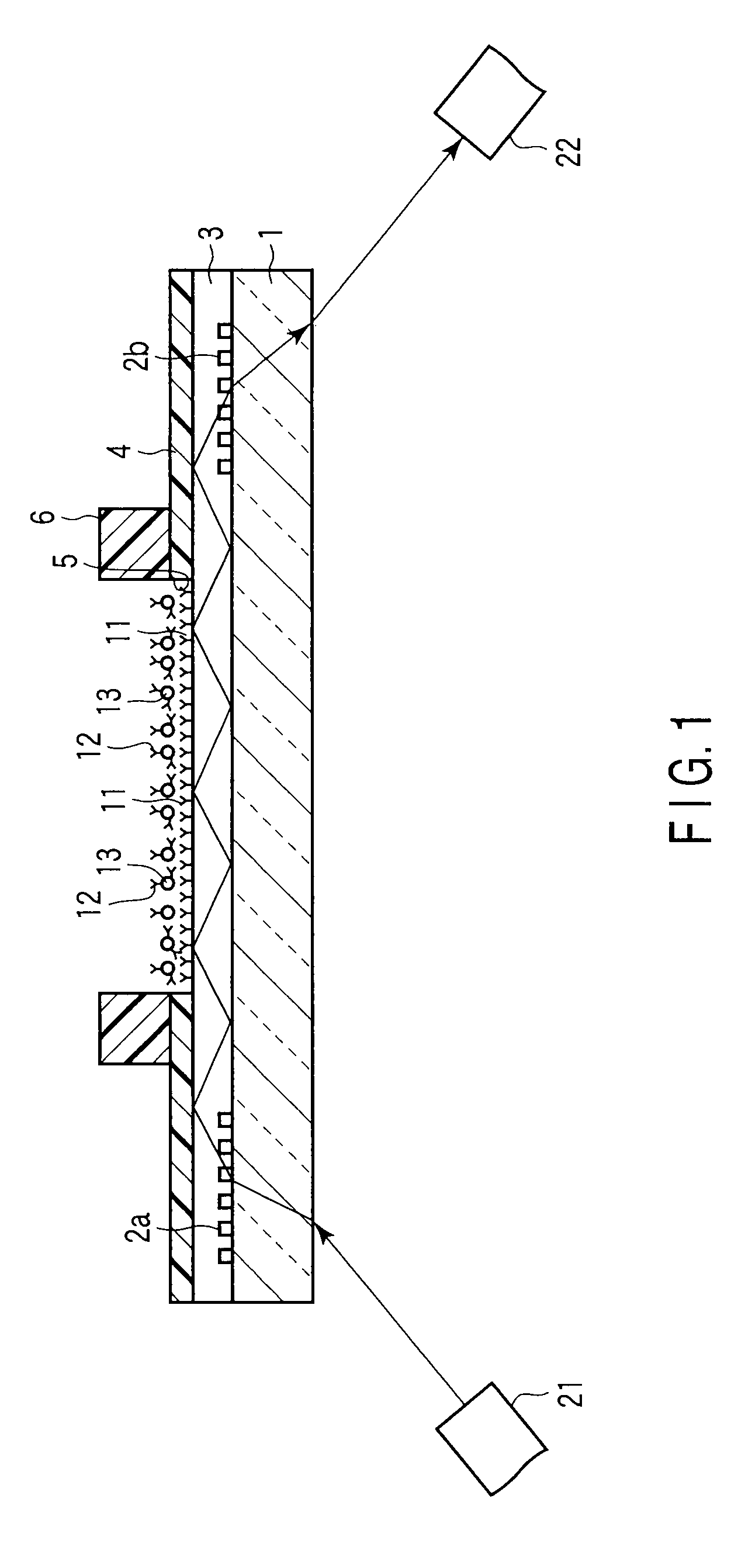
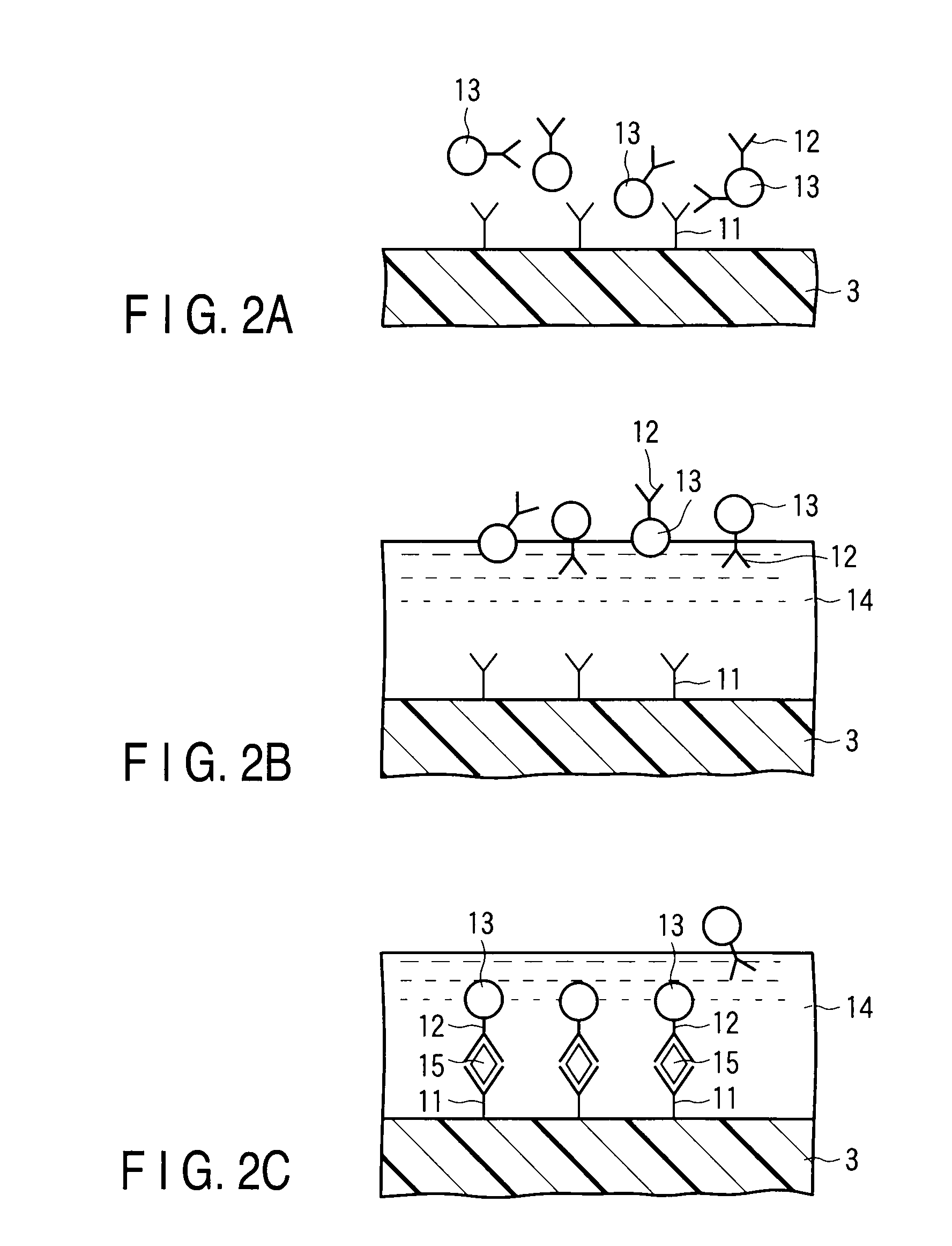
[0087]An optical-waveguide sensor chip in the first embodiment comprises an optical waveguide having a first substance immobilized on the surface thereof.

[0088]The first substance is specifically reactive with an analyte substance. Fine particles are dispersed on the optical waveguide and having a second substance immobilized on the surface thereof. The second substance is specifically reactive with the analyte substance.

[0089]The analyte substances include, for example, blood, blood sera, blood plasmas, biological samples, and proteins, peptides and genes contained for example in foods. Typical examples thereof include, but are not limited to, hapten hormones such as insulin, casein, β-lactoglobulin, ovalbumin, calcitonin, C-peptide, leptin, β-2-microglobulin, retinol-binding protein, α-1-microglobulin, α-fetoprotein, oncofetal antigens, troponin-I, glucagon-like peptides, insulin-like peptides, tumor growth factors, fibroblast growth factors, platelet growth factors, epidermal gro...

second embodiment

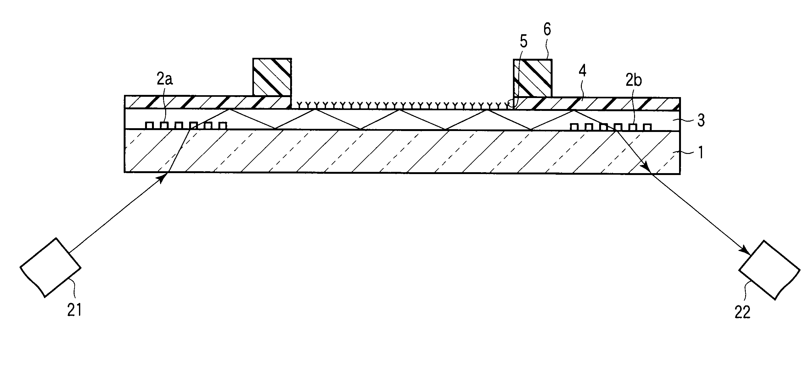
[0111]An optical-waveguide sensor chip in the second embodiment comprises an optical waveguide having a first substance immobilized on the surface thereof. The first substance is specifically reactive with an analyte substance. A supporting plate is placed at a position facing the optical waveguide. Fine particles are dispersed on the surface of the supporting plate facing the optical waveguide. The fine particles have a second substance immobilized on the surface thereof. The second substance is specifically reactive with the analyte substance.

[0112]For example, a planar optical waveguide can be used as the optical waveguide. Similarly to the first embodiment described above, the planar optical waveguide may be formed with a thermosetting resin or a nonalkali glass.

[0113]A first substance which is specifically reactive with an analyte substance in the analyte sample is immobilized on the planar optical waveguide in a manner similar to the method described in the first embodiment. F...

third embodiment

[0131]A method of measuring a substance according to the third embodiment will be described below.

[0132]First, an optical-waveguide sensor chip comprising an optical-waveguide sensor chip comprising an optical waveguide having a first substance immobilized on the surface thereof is prepared. The first substance is specifically reactive with an analyte substance. In addition, a dispersion of fine particles having a second substance immobilized on the surface thereof is prepared. The second substance is specifically reactive with the analyte substance.

[0133]Subsequently, an analyte sample solution is then dropped on the surface of the optical waveguide to allow a specific reaction between the first substance on the optical waveguide and the analyte substance in the analyte sample solution. Then, the surface of the optical waveguide is washed. Subsequently, the dispersion of fine particles is dropped on the surface of the optical waveguide to allow specific reaction between the analyte...


PUM


Abstract

An optical-waveguide sensor chip includes an optical waveguide having a first substance immobilized on the surface thereof, the first substance being specifically reactive with an analyte substance, and fine particles dispersed on the optical waveguide and having a second substance immobilized on the surface thereof, the second substance being specifically reactive with the analyte substance.

Description

CROSS-REFERENCE TO RELATED APPLICATIONS[0001]This application is based upon and claims the benefit of priority from prior Japanese Patent Applications No. 2007-290210, filed Nov. 7, 2007; and No. 2008-274708, filed Oct. 24, 2008, the entire contents of both of which are incorporated herein by reference.BACKGROUND OF THE INVENTION[0002]1. Field of the Invention[0003]The present invention relates to an optical-waveguide sensor chip, a method of manufacturing the optical-waveguide sensor chip, a method of measuring a substance, a substance-measuring kit and an optical-waveguide sensor.[0004]2. Description of the Related Art[0005]Normally in conventional immunological assays by using antigen-antibody reaction, primary antibodies corresponding to the analyte such as protein in the analyte sample are immobilized on the surface of a well-shaped substrate. Particular amounts of an analyte sample solution, a secondary antibody solution, and a coloring reagent are added dropwise to the well s...

Claims


Application Information

Patent Timeline
IPC IPC(8): G01N33/543G01N21/00B05D5/06
CPCG01N21/552G01N21/7703G01N33/54313G01N21/75G02B6/12007G02B6/124G01N33/54373
Inventor KASAI, SHINGOUEMATSU, IKUOTONO, ICHIROTAKASE, TOMOHIRONAWATA, ISAOOOMIYA, KAYOKOOYAMA, YURIKOHONJOH, TSUTOMU
Owner KK TOSHIBA
Why Eureka
Try Eureka