Storage apparatus

Inactive Publication Date: 2009-05-21
GUDENG PRECISION IND CO LTD
View PDF25 Cites 4 Cited by
  • Summary
  • Abstract
  • Description
  • Claims
  • Application Information

AI Technical Summary

Benefits of technology

[0009]Thereupon, it is one objective of the present invention to provide a storage apparatus for storing a semiconductor element or a reticle and having a filter for filtering dust in air so as to protect the reticle or the semiconductor element accommodated therein from being defiled.
[0010]It is another objective of the present invention to provide a storage apparatus for storing a semiconductor element or a reticle and having a filter for filtering the dust in air so as to maintain cleanliness therein.

Problems solved by technology

Since any dust (such as particles, powders or an organic matter) can adversely affect the quality of such projected pattern, the reticle used to produce the pattern on the silicon wafer that is required with absolute cleanness.
However, absolute dustless environment is inaccessible even in known clean rooms.
However, for enhancing the yield of products and reducing manufacturing cost, in addition to meeting the required cleanliness, defilement that is brought to reticles by external gases has to be precluded.
These unexpected gases can cause foggy surfaces of reticles or semiconductor elements that render the reticles or semiconductor elements becoming rejects resulting in wasted manufacturing costs.

Method used


Image

  • Storage apparatus
  • Storage apparatus
  • Storage apparatus

Examples


Embodiment Construction

[0019]While the present invention discloses a storage apparatus for storing a semiconductor element or a reticle and having a filter therein, it is to be stated first of all that the detailed manufacturing or processing procedures of the disclosed storage apparatuses relay on known technology and need not be discussed at length herein. Meantime, while the accompanying drawings are provided for the purpose of illustration, it is to be understood that the components and structures therein need not to be made in scale.

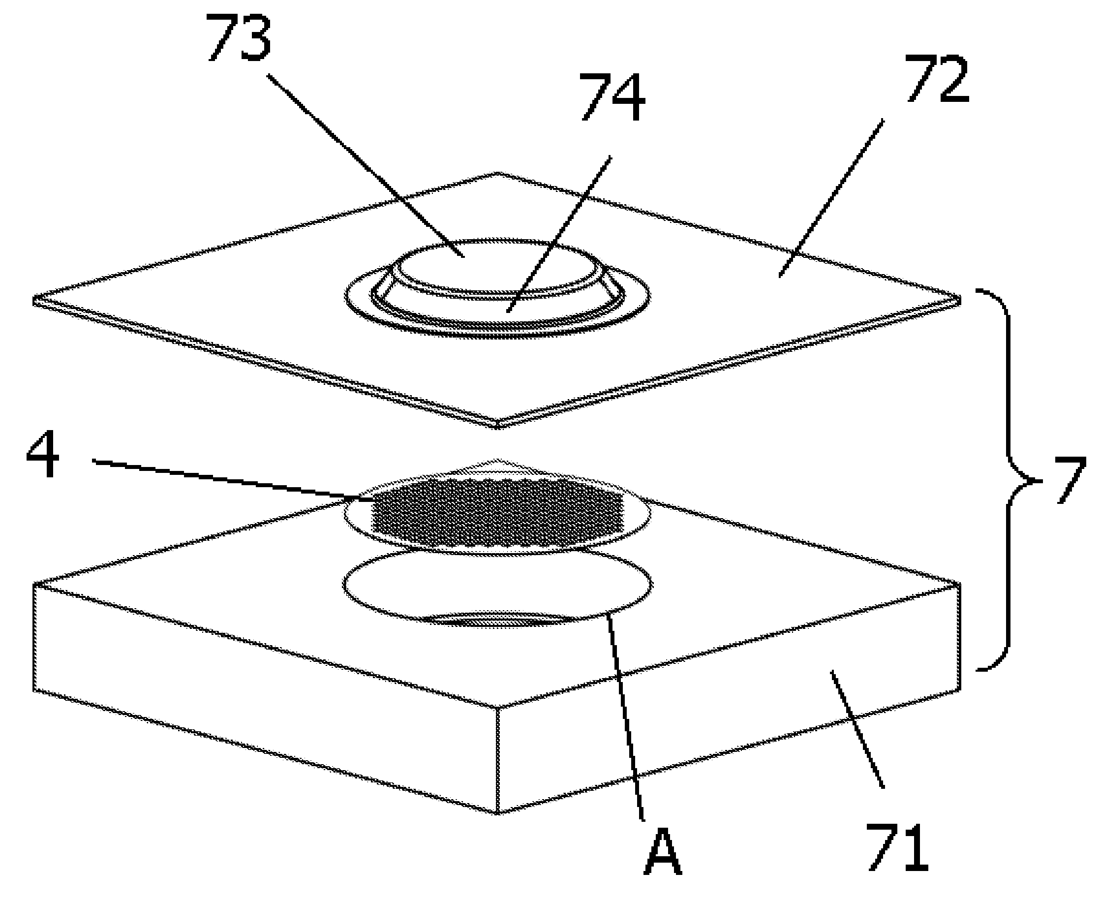
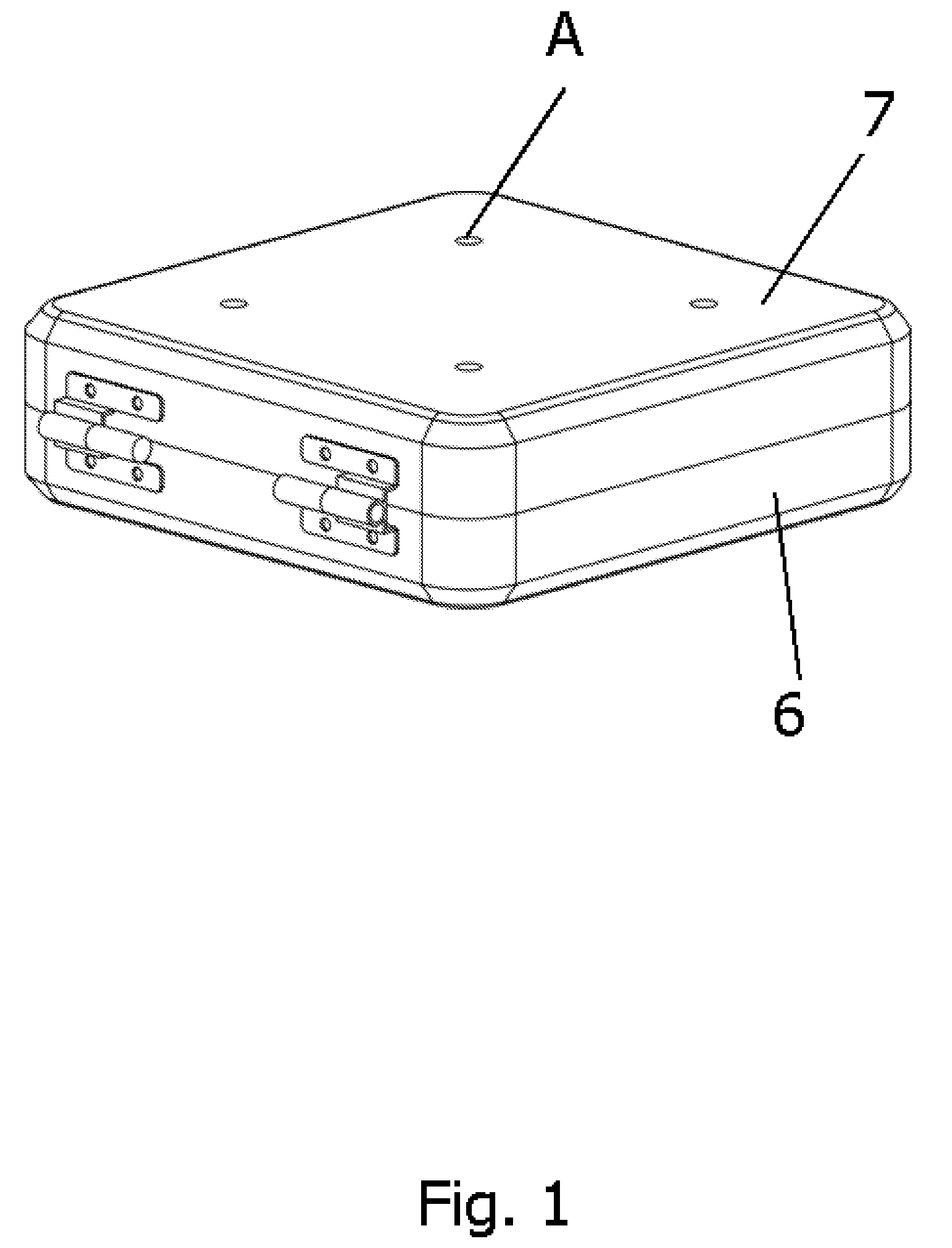
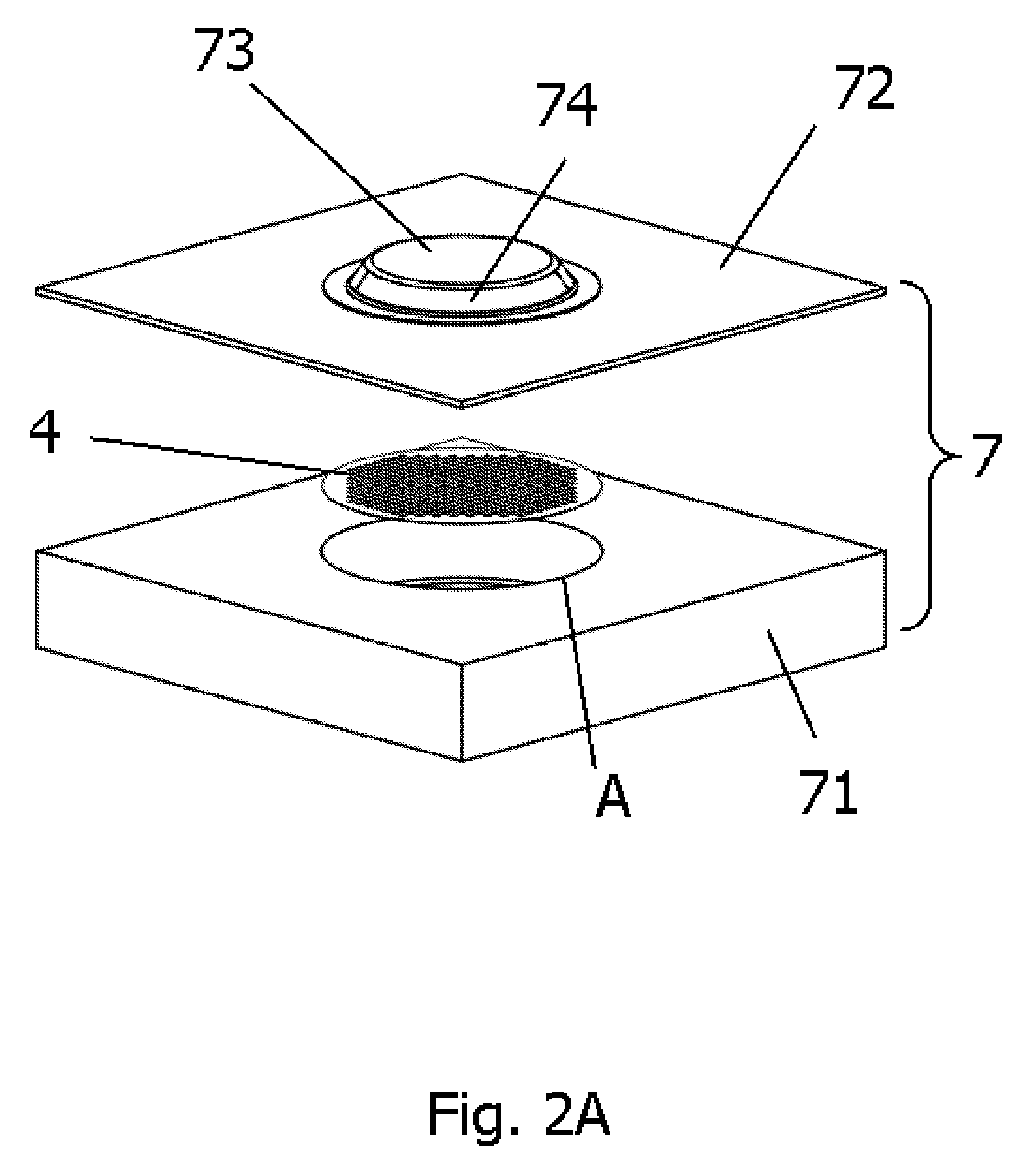
[0020]Please refer to FIG. 1 is a view of a storage apparatus for storing a semiconductor element or a reticle according to the present invention. The storage apparatus includes a first cover 6 and a second cover 7 which are assembled to form an inner space therebetween for accommodating a semiconductor element or a reticle. In this embodiment, the semiconductor element such as FOUP (Front Opening Unified Pod), FOSB (Front Opening Shipping Pod) or any kind of wafer pod. T...


PUM


Abstract

The present invention provides a storage apparatus for storing a semiconductor element or a reticle and having a filter therein. The storage apparatus includes a first cover and a second cover, which are assembled together to form an inner space therebetween for accommodating a reticle or a semiconductor element. The second cover of the storage apparatus is composed of a body and a plate. Further, the second cover includes at least one aperture for communicating the inner space and an outer of the storage apparatus. The plate has a corresponding portion positionally corresponding to the aperture of the body. The filter is sandwiched between the body and the plate and covered the aperture so that when the air passes through the aperture of the body, the filter can filter and rid the air of impurities.

Description

BACKGROUND OF THE INVENTION[0001]1. Technical Field[0002]The present invention relates to storage apparatuses for storing semiconductor elements, or reticles and, more particularly, to a storage apparatus for storing a semiconductor element or a reticle and having a filter.[0003]2. Description of Related Art[0004]In the rapidly developing semiconductor technology, optical lithography plays an important role and wherever pattern definition is conducted, optical lithography is requisite. As to the application of optical lithography relating to semiconductors, a designed circuit pattern is used to produce a light-transparent reticle. Basing on the principle of exposure, after a light passes through the reticle and projects on a silicon wafer, the circuit pattern formed on the reticle can be exposed onto the silicon wafer. Since any dust (such as particles, powders or an organic matter) can adversely affect the quality of such projected pattern, the reticle used to produce the pattern o...

Claims


Application Information

Patent Timeline
IPC IPC(8): B65D85/00
CPCH01L21/67353H01L21/67393H01L21/67359
Inventor WANG, SHENG-HUNG
Owner GUDENG PRECISION IND CO LTD
Why Eureka
Try Eureka