Surface mount package with enhanced strength solder joint

Inactive Publication Date: 2009-05-21
SKYWORKS SOLUTIONS INC
View PDF20 Cites 7 Cited by
  • Summary
  • Abstract
  • Description
  • Claims
  • Application Information

AI Technical Summary

Benefits of technology

[0008]In many industries, including the wireless communications industry, there is an ever-present drive toward smaller and more complex devices such as, for example, smaller cellular telephones that have more features and capability. This, in turn, fuels a drive toward smaller and more complex components. Therefore, semiconductor package manufacturers seek to decrease the pitch of the BGA in order to decrease the package size and/or to increase the interconnection density of the package. In addition, growing environm

Problems solved by technology

While this type of solder joint structure has performed adequately for lead-based solder alloys and coarse pad pitch, it becomes less reliable as pitch decreases, particularly when lead-free solder alloys, which are more brittle than lead-based

Method used


Image

  • Surface mount package with enhanced strength solder joint
  • Surface mount package with enhanced strength solder joint
  • Surface mount package with enhanced strength solder joint

Examples


Example

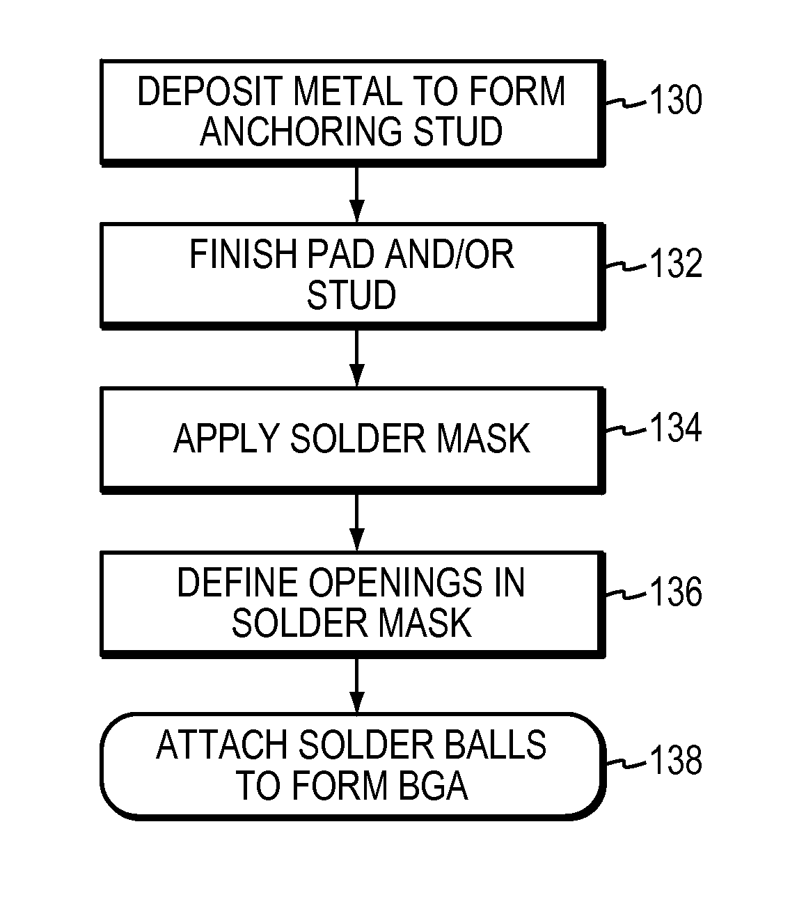
[0021]As discussed above, with the semiconductor industry moving toward smaller components and the growing use of lead-free solder, there is a need for a solder joint structure with improved mechanical integrity. Accordingly, at least some aspects and embodiments are directed to a substrate pad having a plated metal stud that anchors the solder to the pad interface, as discussed below. Pads according to embodiments of the invention may have enhanced structural integrity and particularly, improved ability to withstand mechanical impact, due to the presence of the anchoring metal stud which may provide a more compliant solder joint, even when lead-free solder is used.

[0022]It is to be appreciated that embodiments of the methods and apparatuses discussed herein are not limited in application to the details of construction and the arrangement of components set forth in the following description or illustrated in the accompanying drawings. The methods and apparatuses are capable of imple...


PUM


Abstract

A substrate pad in a semiconductor package having a geometry and structure that facilitates providing a solder joint to the pad that has enhanced structural integrity and resistance to mechanical impact. The pad may include a plated metal stud that anchors the solder to the pad interface, providing a more compliant solder joint, even when lead-free solder is used.

Description

BACKGROUND[0001]1. Field of Invention[0002]The present invention relates generally to semiconductor devices and methods for fabricating the same and, more particularly, to solder joints and pad structures for surface mount semiconductor devices.[0003]2. Discussion of Related Art[0004]Presently, there are several semiconductor packaging techniques that are well received in the radio frequency (RF) component industry. One widely used package is the ball grid array (BGA) type package. BGA is a surface-mount package that utilizes an array of metal spheres or balls to provide external electrical interconnection to the packaged component. The balls are composed of solder, and are attached to a laminated substrate at the bottom side of the package. The die of the BGA is connected to the substrate either by wirebonding or flip-chip connection. The substrate of a BGA has internal conductive traces that route and connect the die-to-substrate bonds to the substrate-to-ball array bonds.[0005]Re...

Claims


Application Information

Patent Timeline
IPC IPC(8): H01L23/48H01L23/52H01L21/02
CPCH01L23/49811H01L2224/32225H01L2224/48091H01L2224/48227H01L2224/73265H01L24/48H01L2924/01079H01L2924/15311H01L2924/30107H01L2924/01078H01L2924/01327H01L2924/00014H01L2924/00H01L2924/14H01L2924/181H01L2924/00012H01L2224/45099H01L2224/45015H01L2924/207
Inventor KIM, PATRICKKUHLMAN, MARK A.GUO, YIFANLOBIANCO, ANTHONYWARREN, ROBERT W.
Owner SKYWORKS SOLUTIONS INC
Why Eureka
Try Eureka