Organic electric field light-emitting display device

a display device and electric field technology, applied in the direction of discharge tube luminescnet screens, discharge tube/lamp details, electric discharge lamps, etc., can solve the problems of high resistance in parts of the power auxiliary circumferential line or a disconnection, contamination may spread, air holes may be formed, etc., to reduce resistance in these portions, prevent air holes, and alleviate height differences

Inactive Publication Date: 2009-05-21
SONY CORP
View PDF7 Cites 13 Cited by
  • Summary
  • Abstract
  • Description
  • Claims
  • Application Information

AI Technical Summary

Benefits of technology

[0019]It is desirable to prevent disconnection of the power auxiliary circumferential line due to a height difference at intersections between the power auxiliary circumferential line and signal or scan lines. It is also desirable to prevent air holes which could cause contamination.
[0028]According to the first embodiment, the plurality of dummy wirings are formed on the underlying layer of the power auxiliary circumferential line. The plurality of dummy wirings are formed between intersections between the power auxiliary circumferential line and at least either one of the plurality of signal lines or the plurality of scan lines. The plurality of dummy wirings are insulated and isolated from the signal or scan lines. This alleviates, by means of the dummy wirings, any height difference on the surface where the power auxiliary circumferential line is formed during the formation thereof, thus providing a more planarized surface. As a result, the power auxiliary circumferential line is resistant to disconnection due to a height difference. In addition, air holes can also be prevented.
[0029]According to the second embodiment, each of the dummy wirings made of a wiring material is connected to the power auxiliary circumferential line on the overlying layer at least at two locations. This allows for formation of a bypass route for transmission of the potential in portions of the power auxiliary circumferential line, thus providing a reduced resistance in these portions. Further, if the resistance becomes higher in these portions of the power auxiliary circumferential line or if the same line disconnects in these portions, the dummy wiring serves as an alternative wiring of the power auxiliary circumferential line, thus ensuring redundancy.
[0030]According to the third embodiment, the plurality of signal lines, the plurality of scan lines and the plurality of dummy wirings at the intersections include at least two conductive layers laminated during the formation of each of the thin film semiconductor layer and gate electrode layer. The thin film semiconductor layer and gate electrode layer make up the TFTs. As a result, the signal or scan lines and dummy wirings can be formed at the same layer level and at the same height, further alleviating the height difference (providing a more flat surface).
[0031]According to the fourth embodiment, the lower layer electrode of the organic EL element, the power auxiliary circumferential line and the power auxiliary grid line (major portion thereof) are formed by the wiring layer at the same layer level. The plurality of signal lines and a plurality of control lines have their ends formed, on an underlying layer, as bridge lines at the same layer level as the dummy wirings for extension. The power auxiliary circumferential line crosses over the bridge lines via the insulating film. Therefore, a wiring layer is used for the power auxiliary circumferential line and power auxiliary grid line. Other than this wiring layer, the (conductive) layer structure of the organic electric field light-emitting display device includes an upper layer electrode layer of the organic EL elements and several other conductive layers such as TFT gate electrode layer and thin film semiconductor layer. Thus, the organic electric field light-emitting display device has a simple conductive layer structure.
[0032]The present invention can effectively prevent disconnection of the power auxiliary circumferential line due to a height difference at an intersection between the power auxiliary circumferential line and signal or scan line. The present invention can also effectively prevent air holes which could cause contamination. This makes it possible to provide a highly reliable organic electric field light-emitting display device with a low defect rate which prevents uneven display and offers high reliability.

Problems solved by technology

This may lead to a high resistance in part of the power auxiliary circumferential line or a disconnection of the same line due to the height difference.
However, there is an undeniable concern that air holes may be formed in the EL protection film due to a height difference and that contamination may spread from these air holes due, for example, to moisture or foreign matter to such an extent that even the pixel section is adversely affected.

Method used


Image

  • Organic electric field light-emitting display device
  • Organic electric field light-emitting display device
  • Organic electric field light-emitting display device

Examples


first embodiment

[0042]

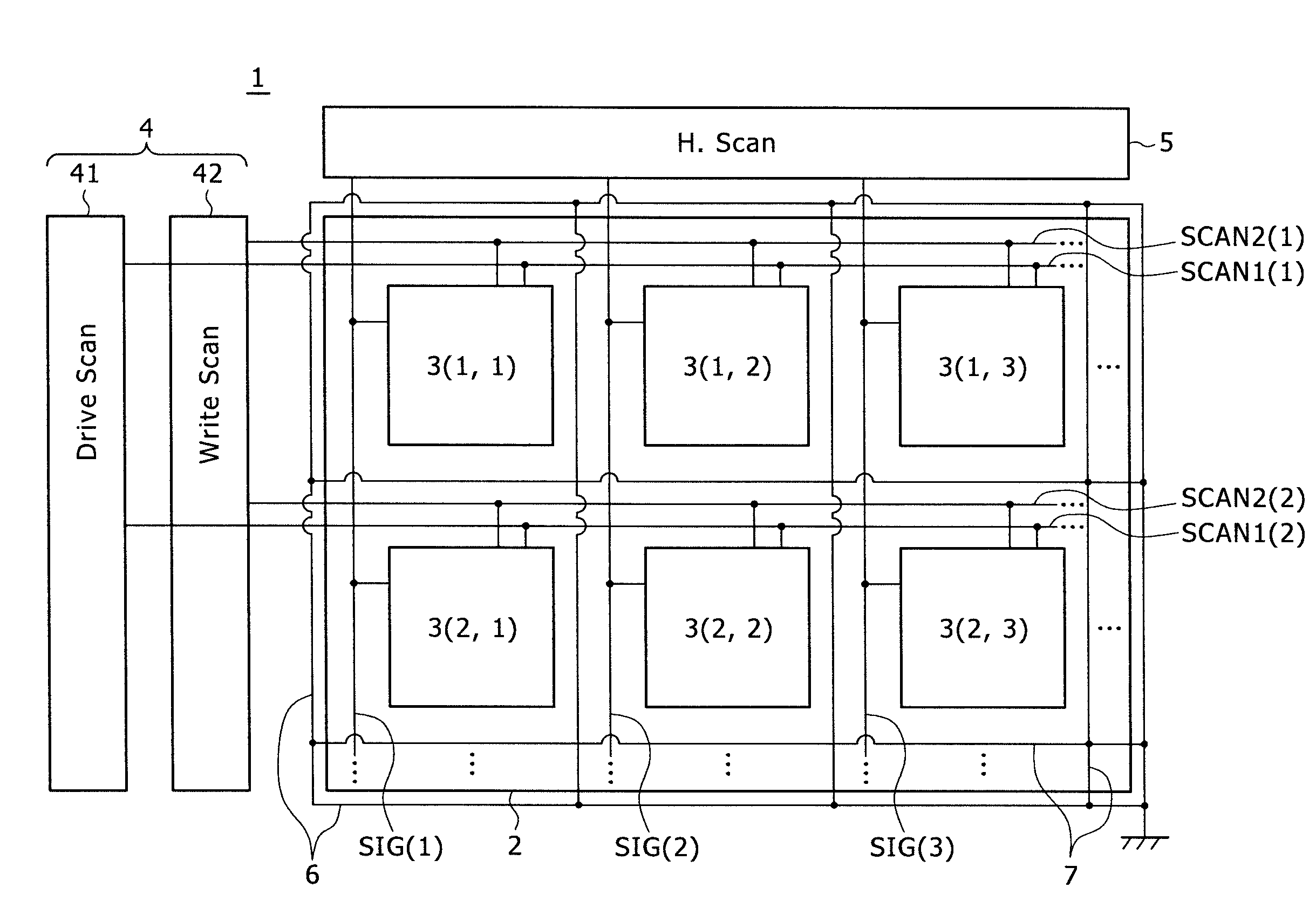
[0043]FIG. 1 illustrates major components of an organic EL display according to embodiments of the present invention.

[0044]An organic EL display 1 illustrated includes a pixel array 2 and drive circuits adapted to drive the pixel array 2. The pixel array 2 has a plurality of pixel circuits 3(i, j) arranged in a matrix. The size of the pixel array 2 defines the “pixel arrangement region.”

[0045]The drive circuits include vertical drive circuits (V. scanners) 4 and horizontal drive circuit (H. scanner: H. Scan) 5.

[0046]The plurality of V. scanners 4 are provided according to the configuration of the pixel circuits 3. Here, the V. scanners 4 are a horizontal pixel line drive circuit (Drive Scan) 41 and write signal scan circuit (Write Scan) 42.

[0047]Reference numerals 3(i, j) of the pixel circuits shown in FIG. 1 mean that each of the circuits has a vertical address i (i=1 or 2) and horizontal address j (j=1, 2 or 3). These addresses ‘i’ and ‘j’ take on an integer value of 1 or la...

second embodiment

[0120]The second embodiment differs from the first embodiment in the configuration around the dummy wiring DL. Therefore, FIGS. 1 to 5 and description thereof for the first embodiment also apply to the second embodiment.

[0121]FIG. 7 illustrates a sectional view taken along line A-A in FIG. 5 according to the second embodiment of the present invention.

[0122]FIG. 7 differs from FIG. 6 in that contacts 12M1 and 12M2, each including a first contact hole (1CH), are provided at each end of the dummy wiring DL, and that the two ends of the dummy wiring DL are connected to the rear surface of the power auxiliary circumferential line 6 by means of the contacts 12M1 and 12M2. The second embodiment is the same as the first embodiment in other configuration.

[0123]It should be noted that the EL protection film 21 is omitted in FIGS. 6 and 7.

modification example

[0124]FIGS. 5 to 7 illustrate the intersections between the power auxiliary circumferential line 6 and first and second scan lines SCAN1(i) and SCAN2(i), with the dummy wiring DL disposed between the intersections and along the same line 6.

[0125]The similar dummy wiring DL may be disposed on the underlying layer between the intersections between the power auxiliary circumferential line 6 and signal lines, i.e., signal lines SIG(j), and along the same line 6. Further, the dummy wiring DL may be disposed not only between the intersections between the power auxiliary circumferential line 6 and scan lines but also between the intersections between the same line 6 and signal lines. In this case, either of the sectional structures shown in FIGS. 6 and 7 may be used.

[0126]In the second embodiment, it suffices to form at least one contact at each end of the dummy wiring DL or a total of two contacts for connection between the dummy wiring DL and power auxiliary circumferential line 6. There...


PUM


Abstract

An organic electric field light-emitting display device includes: a plurality of pixel circuits, each disposed at one of the intersections between a plurality of signal lines and a plurality of scan lines, each of the pixel circuits including an organic electric field light-emitting element; a power auxiliary circumferential line electrically connected to one of two electrodes adapted to apply an electric field to the organic electric field light-emitting element, the power auxiliary circumferential line being disposed in a ring-like arrangement around the pixel arrangement region; and a plurality of dummy wirings formed on the underlying layer of the power auxiliary circumferential line between the intersections between either one of the plurality of signal lines and the plurality of scan lines and the power auxiliary circumferential line, the plurality of dummy wirings being insulated and isolated from the signal or scan line in proximity.

Description

CROSS REFERENCES TO RELATED APPLICATIONS[0001]The present invention contains subject matter related to Japanese Patent Application JP 2007-296572 filed in the Japan Patent Office on Nov. 15, 2007, the entire contents of which being incorporated herein by reference.BACKGROUND OF THE INVENTION[0002]1. Field of the Invention[0003]The present invention relates to an organic electric field light-emitting (EL) display device having, for each pixel, an organic electric field light-emitting (EL) element adapted to emit light when a current flows through its organic multilayer film between two electrodes as a result of application of an electric field between the two electrodes.[0004]2. Description of the Related Art[0005]An organic EL display device (organic EL display) has a display panel which includes a display section and drive section of the display section. The display section has a plurality of pixel circuits arranged in a matrix. The display panel is manufactured by forming the disp...

Claims


Application Information

Patent Timeline
Patent Type & Authority Applications(United States)
IPC IPC(8): H01J1/62
CPCH01L27/3276H01L27/3223H10K59/88H10K59/131H01L2924/13069H10K50/11
Inventor SAGAWA, HIROSHIUCHINO, KATSUHIDE
Owner SONY CORP
Why Eureka
Try Eureka